1、What is microanalysis technology
With the continuous advancement of science and technology, micro-area analysis technology has been widely used. This technology can analyze and characterize the chemical composition, structure, and physical properties of tiny particles, accurately revealing the characteristics and mechanisms of matter. In fields such as medicine, life sciences, earth sciences, and materials science, microanalysis technology plays an important role.
The emergence of microanalysis technology originated in the early 20th century. At that time, using electron microscopy (SEM) to observe different parts of some substances had become a common analysis method. With the continuous development of SEM, it was discovered that a local area ofthe sample can be heated intensively, thereby completely oxidizing. Adhering to the principles of analytical chemistry, this method is called electron probe microanalysis (EPMA). This technology can accurately determine and quantify the volume fraction and micro-area chemical composition of various elements and has now become one of the basic tools in materials science, earth science, and environmental science research.
Another micro-analysis technology is field emission scanning electron microscopy (FE-SEM) and transformed thermosensitive fluorescent probe (TMA) technology. The emergence of these two technologies has brought new heights that cannot be achieved by electron probe micro-analysis technology. It can not only obtain information on chemical elements but also reveal information on crystal grain boundaries and interfaces in materials.
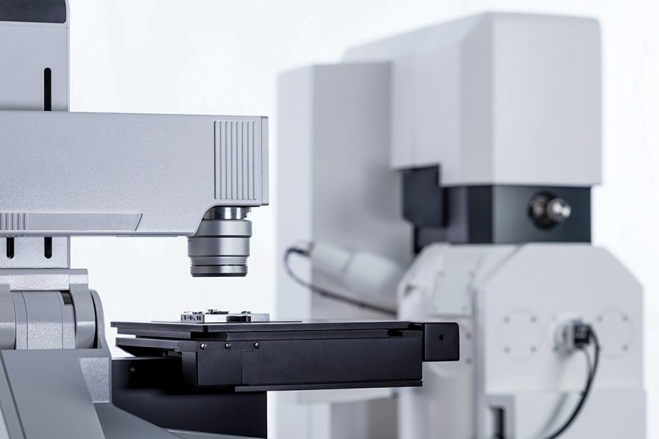
Microanalysis technology refers to the technology that uses a series of technologies/principles to analyze the surface morphology, element content and form of objects with tiny physical dimensions that exceed the resolution of the human eye. In integrated circuit failure analysis, commonly used microanalysis techniques include optical microscopes and X-ray photoelectron spectroscopy with photon beams as the incident beam, scanning electron microscopes, transmission electron microscopes, Auger electron spectroscopy and X-ray microanalysis technology, focused ion beam (FIB) with ion beam as the incident beam, secondary ion mass spectrometry and scanning probe technology, such as scanning tunneling microscope, atomic force microscope, scanning capacitance microscope, scanning thermal microscope, scanning near-field microscope and atomic force probes, etc.
Microanalysis technology plays an indispensable role in integrated circuit failure diagnosis and material characterization. It is one of the most basic and most widely used equipment in analytical laboratories.
2、The four most widely used microscopes for microanalytical techniques
(1) Optical microscope:
Features: simple operation, intuitive graphics;
System composition: An optical microscope generally consists of a condenser illumination system, objective lens, eyepiece (optical system) stage, focusing mechanism (mechanical system), and camera system.
Resolution: micron level. Generally, the maximum magnification of the objective lens is 160x or 200x; the magnification of the eyepiece is 10x. Therefore, the maximum magnification of the microscope is 1600x or 2000x. The resolving power of the human eye in its natural state is about 0.25 μm, and the maximum resolving power of the microscope is 0.16 μm or 0.13 μm. It can be found that the resolution limit of the microscope can no longer meet the resolution requirements for deep submicron IC structure analysis.
Wafer inspection microscope (manual)
- Mainly used for wafer shipment quality inspection or die screening;
- Lamp source: halogen lamp;
- Transfer method: manually place the sample, the sample can be a wafer or a die;
Microscopic examination pictures
Wafer inspection microscope (automatic)
- Mainly used for front-end/back-end wafer defect detection;
- Automatic film transfer by machine;
- More functions can support multi-layer partition detection, algorithm support, and SEM functions.
(2) Scanning electron microscope (SEM):
Principle: The working principle of a scanning electron microscope is as shown in the figure. The top electron light source (commonly called an electron gun) emits electrons. Under the action of an accelerating voltage (usually 200V~30KV), the electrons pass through two or three electromagnetic lenses and condense into a very thin beam of electrons. The incident electron beam is driven by the scanning coil above the objective lens to perform orderly raster scanning on a small area on the surface of the sample.
After the high-energy electron beam is incident on the sample, it will stimulate various information such as secondary electrons, backscattered electrons, X-rays and Auger electrons on its surface. This information is detected by corresponding detectors, amplified and transmitted to the display screen to modulate the brightness of the display screen. Scanning electron microscopy uses this line-by-line scanning and point-by-point imaging method to convert different information features on the sample surface into video signals in sequence and proportion so that we can observe the features corresponding to the sample surface on the fluorescent screen. Magnified microscopic topography image.
SEM system diagram
The scanning electron microscope mainly analyzes the morphology information and composition information of the sample by detecting secondary electrons and backscattered electrons. It can also be connected to an energy spectrometer to analyze the composition of the sample by collecting X-rays.
Secondary electrons are extranuclear electrons that are bombarded by the incident electron beam and leave the sample surface. They mainly come from the depth range of 1~10nm on the sample surface and have low energy (0~50eV, average 30eV), so the secondary electron image can be well Shows the microscopic morphology of the sample surface. Since the incident electrons only pass through a path of a few nanometers and have not been reflected multiple times and significantly diffused, the secondary electron area generated in the action area irradiated by the incident electrons is not much different from the beam spot diameter of the incident beam, so the beam spot diameter on the same station Secondary electron images have the highest resolution among electron microscopes. . The resolution of a scanning electron microscope is generally the secondary electron resolution.
Backscattered electrons are part of the electrons bounced back from the atoms in the solid sample (the energy is greater than 50eV, less than the incident electron energy E0, most of which is about 0.7~0.9E0). Under a certain accelerating voltage, the yield of backscattered electrons increases with the increase of the atomic number of the sample. Therefore, the backscattered electron signal can not only analyze the morphological characteristics of the sample, but also display the chemical composition characteristics of the sample, and roughly conduct a qualitative analysis of the chemical composition distribution on the sample surface within a certain range.
Resolution: Cold field emission electron microscope, when the accelerating voltage is 15kV, it can reach 1.5nm; S-5200, when the accelerating voltage is 30kV, it can reach 0.5nm.
Common SEM pictures
(3) Transmission electron microscope (TEM)
TEM is the technology with the highest resolution among all microanalytical technologies and has become an indispensable daily analysis and observation tool in analytical laboratories in the era of deep submicron dimensions. Taking the FEI T20 field emission transmission electron microscope as an example, the three main indicators of currently commercial transmission electron microscopes are as follows: ① Acceleration voltage: 200kV. The accelerating voltage of commonly used TEM is in the range of 200 to 40kV. ②Resolution: point resolution=0.248nm; line resolution=0.102nm. ③Magnification: The maximum magnification of modern TEM is about one million times.
System composition:
Electron Gun: Emits electrons. It includes cathode, grid and anode. The electrons emitted from the cathode tube pass through the grid aperture to generate a ray beam, which is accelerated under the anode voltage and then incident into the condenser mirror, where it plays the role of accelerating the electron beam and pressurizing the electron beam.
Concentrator: Concentrates the electron beam to obtain a parallel light source.
Sample holder: Load the sample to be observed.
Objective lens: focused imaging, one-time magnification.
Intermediate mirror: secondary magnification and control of imaging mode (image mode or electron diffraction mode).
Projection mirror: three times magnification. l Fluorescent screen: converts electronic signals into visible light for the operator to observe.
CCD camera: Charge-coupled element that converts optical images into digital signals.
Schematic diagram of the basic structure of a transmission electron microscope
Sample delivery requirements:
- The size of a single powder is preferably less than 1μm;
- Non-magnetic;
- Mainly inorganic components, otherwise it will cause serious pollution of the electron microscope, high voltage jump, and even damage the high voltage gun;
- The block needs electrolytic thinning or ion thinning to obtain a thin area of tens of nanometers before observation; if the grain size is less than 1 μm, powder can also be made into powder by mechanical methods such as crushing for observation;
TEM is mainly used for the analysis and research of the microstructure and micro-region composition of inorganic materials. The functions of the instrument include:
- Electron diffraction: selected area diffraction, micro-beam diffraction, convergent beam diffraction;
- Imaging: bright field image (BF), dark field image (DF), diffraction image, high-resolution image (HREM), scanning transmission image, circumferential angle dark field image (HAADF);
- Micro-area components: point, line, and surface analysis of EELS and EDS energy spectra;
Application scope:
(1) Material scope: any inorganic materials except magnetic materials, including powders, films and blocks; not suitable for organic and biological materials. (2) Scope of characterization: microscopic morphology, particle size, micro-region composition, element distribution, element valence state and chemical bonding, crystal structure, phase composition, structural defects, grain boundary structure and composition, etc.
TEM common functions
As integrated circuits develop to deep sub-micron sizes, some key dimensions have been accurate to nanometers or even several angstroms. The resolution of SEM can no longer meet the requirements for describing ultra-fine structural features. TEM has become a daily observation in modern IC failure analysis laboratories. tool.
Unfortunately, focused ion beam bombardment of the sample surface causes inevitable damage to the sample surface. The surface of the thin film sample caused by ion damage is amorphous, which weakens the contrast during TEM observation. Nowadays, the advanced low accelerating voltage FIB has an accelerating voltage adjustable from the conventional 30kV to 5kV.
The low dielectric constant and porous media introduced in the deep submicron advanced process are particularly susceptible to ion damage during TEM sample preparation. The advent of low acceleration voltage FIB has greatly alleviated this problem.
(4) Focused ion beam
Working principle and structure of focused ion beam: The FIB system mainly consists of the ion source, ion optical system, secondary particle detector, vacuum system, and auxiliary gas system. Commercial models include single beam and dual beam (ion beam + electron beam).
The ion source of the current commercial system is the Liquid Metal Lon Source (LMIS), and the metal material is Gallium (Ga), because the gallium element has a low melting point, low vapor pressure, and good antioxidant power. The ion optical system mainly includes an electrostatic lens system for focusing imaging, a beam plummet, an astigmatism absorber, a mass analyzer, and a beam deflector.
The auxiliary gas system refers to the introduction of different types of auxiliary gases into the FIB, which can achieve the following two main purposes:
- ① Assisted gas etching: by introducing certain reaction gases, such as Cl2, I2, Br2, etc., the target material can be changed The binding energy of the surface may directly react chemically with the target surface, thereby greatly increasing the sputtering yield of the ion beam.
- ②Induced deposition: Depending on the materials required to be deposited, different induction gases are selected, such as W (CO) 6, WF6, Al (CH3) 3, etc. The induced gas is adsorbed on the surface of the solid material in the form of a monomolecular layer. The bombardment of the incident ion beam causes the adsorbed gas molecules to decompose, leaving the metal material on the solid surface. Gas-assisted gas deposition conductors commonly used in commercial FIB systems, such as tungsten or platinum, are mainly used for metal wire connections and test bond growth in IC failure analysis.
The principle of FIB is similar to that of SEM. The main difference is that FIB uses an ion beam as the incident source. The external electric field of FIB acts on the liquid metal ion source, causing the liquid metal or alloy to form a small tip. Coupled with the technology or alloy of negative electric field pulling the tip, The ion beam is derived, and focused through an electrostatic lens, changes the size of the ion beam is through a series of variable apertures, and then uses a mass analyzer to screen out the desired ion species. Finally, the ion beam is focused on the sample through an octupole deflection device and an objective lens and scanned. The beam bombards the sample, producing secondary electrons and ions that are collected as the source of the image, or physical collisions are used to achieve cutting.
The dual-beam FIB system uses electron beams to observe the image when cutting with ion beams. In addition to preventing the ion beam from continuing to “damage the scene”, it can also effectively improve the image resolution. Commercial field emission dual-beam focused ion beam systems, such as FEI Dual-beam 835, have scanning electron microscope resolutions up to 3nm. At the same time, it can also be equipped with an X-ray energy spectrometer or (secondary ion mass spectrometer) for elemental analysis. The diverse analysis functions greatly increase the convenience and usage of the focused ion beam microscope.
Basic functions of a focused ion beam microscope:
- Precisional cutting: The physical collision of ions is used to achieve the purpose of cutting. Widely used in cross-section processing and analysis of integrated circuits (ICs) and LCDs.
- Selective material evaporation (selective deposition): Use the energy of an ion beam to decompose organic metal vapor or gas phase insulating material, and deposit conductors or non-conductors in local areas. It can provide metal and oxide layer deposition (metal and TEOS deposition). ), common metal depositions include platinum (Pt) and tungsten (Tungstun, W), which are used in circuit repair, design error correction, etc.
- Enhanced etching or selective etching (enhanced etching-iodine/selective etching-XeF2): supplemented by corrosive gas to accelerate cutting efficiency or perform selective material removal during line repair.
- FIB can also generate secondary electrons, so FIB can also use PVC technology, and the mechanism is the same as that of SEM voltage contrast. Focused ion beam (FIB) has many unique and important functions and has been widely used in the semiconductor industry. Its characteristic is that it can solve many difficult, time-consuming or simply impossible problems in semiconductor design, manufacturing, inspection, and failure analysis. Problems are solved one by one. For example, circuit repair and layout verification, component failure analysis, production line process anomaly analysis, IC process monitoring – such as photoresist cutting, transmission electron microscope sample production, etc.
FIB common functions