1. What is an electron microscope and its types?
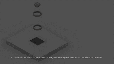
An electron microscope is a microscope that uses an electron beam as the illumination source. They use electron optics similar to the glass lenses of light microscopes to control electron beams, such as focusing them to produce magnified images or electron diffraction patterns. Because the wavelength of electrons is 100,000 times smaller than the wavelength of visible light, electron microscopy has a much higher resolution of about 0.1 nm, compared to the resolution of an optical microscope of about 200 nm. Electron microscopy may refer to:
- Transmission electron microscopy (TEM), where fast electrons pass through thin samples
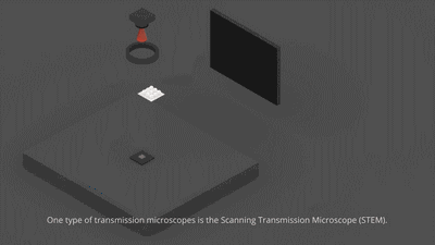
- Scanning transmission electron microscope (STEM) similar to TEM with scanning electron probe
- Scanning electron microscopy (SEM) is similar to STEM, but the sample is thicker
- Electron microprobe is similar to SEM but is more used for chemical analysis
- The ultrafast scanning electron microscope, a very fast version of SEM
- Low energy electron microscopy (LEEM) for surface imaging
- Photoemission electron microscopy (PEEM) is similar to LEEM and uses photons to emit electrons from a surface
2. Four major electron microscopes and their advantages
I believe everyone is familiar with the four major microscopy equipment: SEM, TEM, AFM, and STM, especially those who study materials.
So how do they work? Below, I share with you some awesome animations and pictures to help you easily understand how they work.
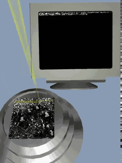
01 Scanning electron microscope (SEM)
SEM – Scanning Electron Microscope: SEM is a microscope that uses an electron beam to scan the surface of a sample and produce an image. Through the interaction between the focused electron beam and the sample, SEM can generate high-resolution images of surface topology and provide information about the sample morphology, composition, and structure.
SEM modulates imaging by using various physical signals excited by finely focused electron beams when scanning the surface of the sample.

SEM uses a point-by-point imaging method to convert different characteristics of the sample surface into images in sequence and proportion, such as secondary electron images.
Backscattered electron images, etc.
The advantages of scanning electron microscopy are:
- (1) Has a higher magnification;
- (2) It has a large depth of field, a large field of view, and a three-dimensional image.
- (3) Sample preparation is simple.
Example pictures:
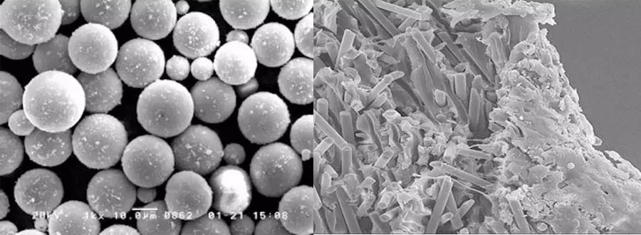
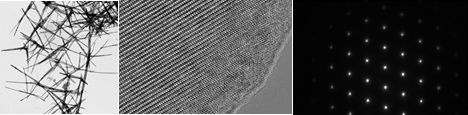
02 Transmission electron microscope (TEM)
TEM – Transmission Electron Microscope: TEM is a microscope that can observe the internal structure of a sample through a thin section of the sample. In a TEM, an electron beam passes through a sample and forms a transmitted electron image. By observing these images, high-resolution information on the internal structure and crystal structure of the sample can be obtained. TEM projects a focused electron beam onto a very thin sample and analyzes the microstructure inside the sample through the image formed by the transmitted electron beam or the diffracted electron beam.


TEM is often used to study the crystallization of nanomaterials, observe the morphology and dispersion of nanoparticles, and measure and evaluate the particle size of nanoparticles.
Example pictures:
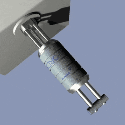
03 Scanning Tunneling Microscope (STM)
STM – Scanning Tunneling Microscope: STM is a microscope that uses the electron tunneling effect to observe the atomic structure of the sample surface. STM works by applying a small voltage between the probe and sample and measuring the current. By adjusting the height of the probe, high-resolution atomic-level surface topology images can be generated and the electronic properties of the sample can be studied. STM is an instrument that uses the tunneling effect in quantum theory to detect the surface structure of matter. A probe carrying a small electrical charge is slowly passed through the material, and a current flows from the probe, through the entire material, to the underlying surface. As the probe passes over individual atoms, the amount of current flowing through the probe fluctuates to create a picture.


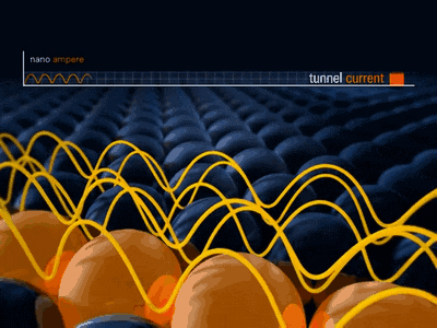
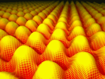
Example pictures:
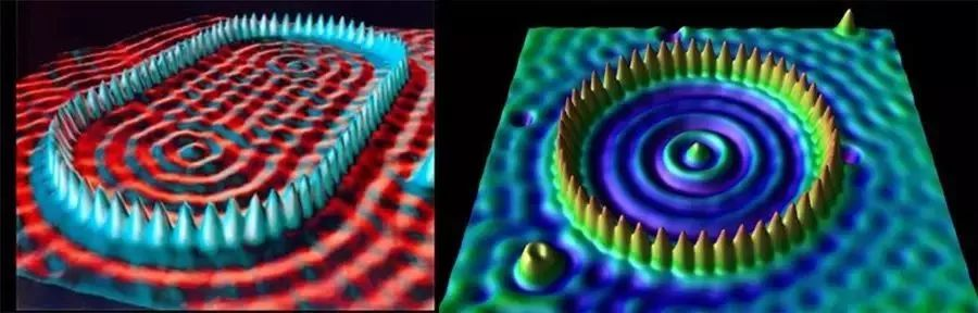
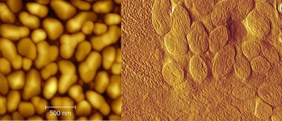
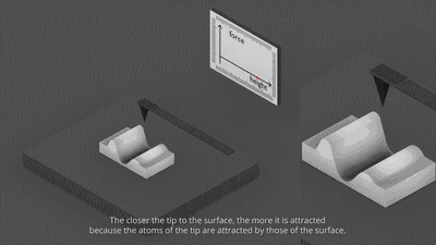
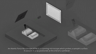
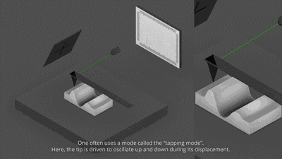
04 Atomic force microscope (AFM)
AFM (Atomic Force Microscope) – Atomic force microscope: AFM is a microscope that uses a scanning probe to detect the topological and mechanical properties of the sample surface. By applying tiny forces between the probe and sample and measuring the probe’s amplitude and feedback signal, AFM can create high-resolution images of surface topology and study the nanoscale properties of the sample. AFM studies the surface structure and properties of substances by detecting extremely weak interatomic interactions between the sample surface and a miniature force-sensitive element. One end of a pair of micro-cantilevers that are extremely sensitive to weak force is fixed, and the tip of the other end is close to the sample. Through their interaction, the micro-cantilevers are deformed or their motion state is changed. Sensors are used to detect these changes to obtain surface topography structure information and surface roughness information.
AFM is divided into contact type, non-contact type, and tapping type.
Advantages of Atomic Force Microscopy:
- (1) AFM provides a true three-dimensional surface map.
- (2) Will not cause damage to the sample.
- (3) Wider applicability.
Example pictures: