TEM and SEM both emit electrons to observe the structure of the sample, but TEM electrons must penetrate the sample to observe its internal lattice, defects, and other information. Wavelength is the determining factor of the resolution of a lens, and the wavelength of the electron beam is inversely proportional to the acceleration voltage. TEM is an electron optical analysis technique that uses an extremely short wavelength electron beam with high acceleration voltage (usually 50-200kV) as the light source, an electromagnetic field as the lens and focuses imaging with high resolution (up to 0.05nm), and magnification up to millions of times.
The first step in being able to associate the functions of a certain material in a device is to gain a deeper understanding of the structure and morphology of the material. This article introduces characterization techniques for the study of ZnO and CuO nanostructures, as well as some details of the electrical and optoelectronic measurements of LED and electrochemical sensor devices. The control principles of each technology were introduced, followed by experimental results, and explained in the discussion section.
1 Scanning Electron Microscope (SEM)
Scanning electron microscopy (SEM) is widely used in various scientific fields to characterize nanomaterials and nanostructures, and is an excellent technology for studying nanoscale surface morphology. By using SEM, it is usually possible to distinguish features at 10nm or smaller scales. Imaging nanostructured materials using SEM usually does not require complex sample preparation (samples only need to be conductive and vacuum-compatible). The basic working principle of SEM is shown in the schematic diagram in Figure 1. SEM uses electrons instead of light to generate images, and electron beams are focused and scanned on selected areas on the surface of the studied sample, hence it is called a scanning electron microscope. In SEM, when an electron beam impacts a sample, a large number of signals are generated. According to the type of detector, the detected signal is converted into an image of the surface morphology of the sample or its components. I used SEM to study the morphology and size of ZnO and CuO nanostructures. For this purpose, secondary electron detectors are used.

The typical energy of secondary electrons is 3-5 eV, and they can only escape from the nano depth of the material surface, depending on the acceleration voltage and the surface density of the sample. Secondary electrons are mainly used for visualizing surface texture/morphology and roughness, as they can accurately mark the position of the beam on the sample surface and provide high-resolution morphology information.
Figure 2 (af) shows SEM images of various morphologies of ZnO nanostructures synthesized under different hydrothermal conditions, with (g) showing SEM images of CuO nanostructures and (h) showing ZnO/CuO hybrid nanostructures synthesized using hydrothermal methods under different conditions.
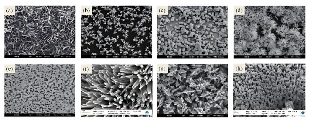
Figure 2: SEM images of ZnO nanostructures;(a) nanorods on Si substrate at neutral pH= 6.6, (b) star-like nanostructures at pH =10, (c) flower-like nanostructures at pH =11, (d) urchin-like nanostructures at pH =12, (e) nanotubes grown on Si substrate, (f) nanorods grown on a paper substrate. (g) shows the SEM image of CuO nanostructures and (h) shows the nanohybrid structures of ZnO/CuO
Along with other characterization techniques, this provides us with information on the morphology, size, and crystallinity of nanostructures.
2 Transmission Electron Microscope (TEM)
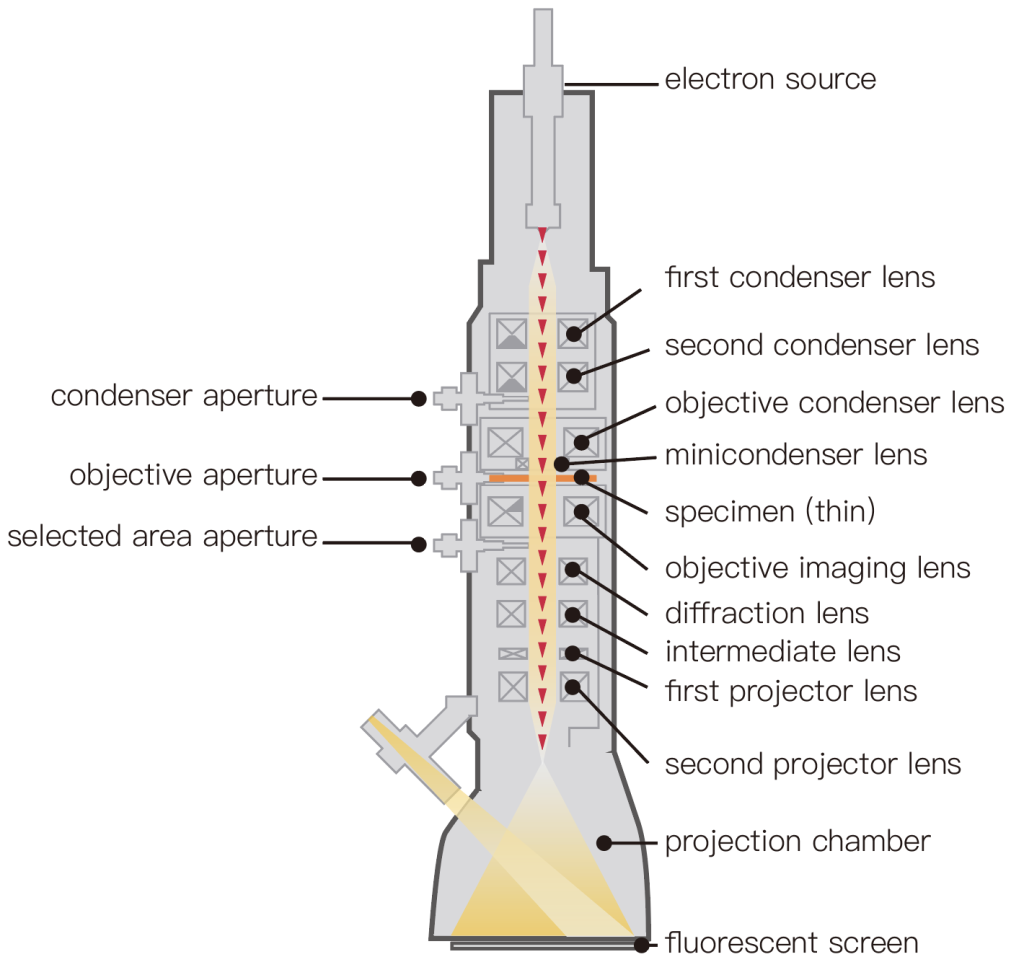
Transmission electron microscopy (TEM), like SEM, belongs to the category of electron microscopes. The basic principle of TEM is similar to that of an optical microscope, except that a high-energy electron source (200 keV) is used instead of light, and a magnetic lens is used instead of a glass lens. TEM is a valuable instrument for characterizing materials, as it can provide imaging with a resolution of several angstroms and crystallographic and chemical information depending on the operating mode. Atomic scale resolution can be obtained through the Rayleigh criterion; The minimum distance resolved is proportional to the wavelength of the radiation used.
Therefore, high-energy electrons with de Broglie wavelengths in the sub-angstrom range can provide atomic resolution. The basic working principle of TEM is shown in the schematic diagram in Figure 3. Unlike SEM, sample preparation in TEM imaging is very cumbersome. The reason is that the electron beam passes through the sample, which means that the sample must be electron transparent, i.e. very thin. To achieve this, in some cases, it is necessary to carefully prepare the sample using polishing and etching. However, I prepared the sample by dispersing the nanostructure in ethanol and casting Drop onto a copper mesh, which is a relatively simple method.
When the electron beam used in TEM passes through the studied sample, the electron beam interacts with the sample, resulting in electron scattering. The number of undispersed electrons passing through a specific part of the sample depends on the scattering potential and thickness of that specific part of the sample. These scattered electrons are collected by the detector and provide the contrast of the sample image, where the change in darkness is determined by the change in density. By observing scattered electrons, diffraction patterns can be obtained, providing information about the crystal structure of the sample. Some papers in this paper have used transmission electron microscopy for material characterization.
Single ZnO nanorods were characterized using TEM (Figure 4). This image indicates that ZnO nanorods have a high-quality single crystal structure and follow the [001] growth direction (right inset in Figure 4). The corresponding selected area electron diffraction (SAED) further demonstrated the single crystal properties and [002] growth direction of ZnO nanorods (Figure 4, left inset).
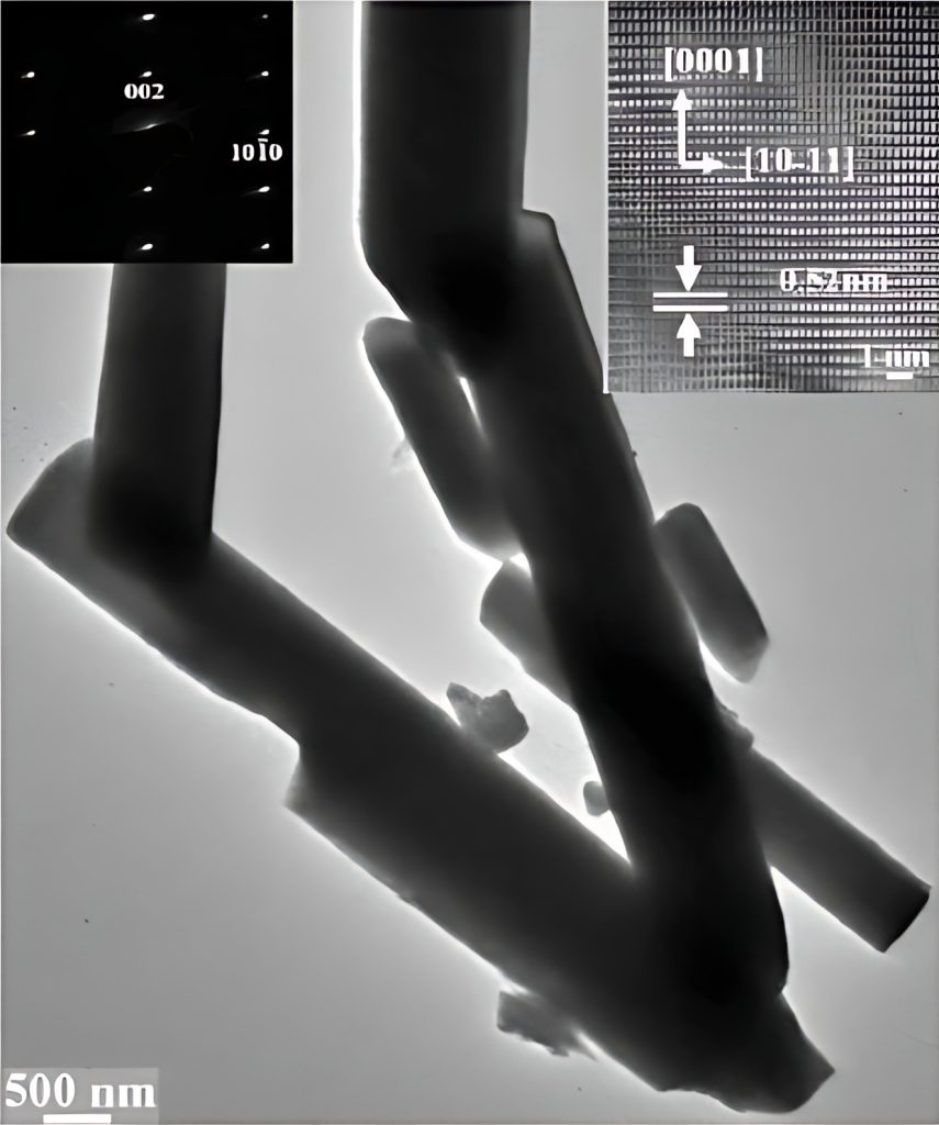
Figure 4: TEM image of the ZnO nanorods, inset (right) shows HRTEM image of the individual nanorods while inset (left) shows the corresponding SAED pattern
Cluster morphology was observed during the growth process, which is also shown in the image, indicating that in solution methods, multiple nanorods often grow out of other nanorods.
The morphology and crystal structure of the grown CuO nanopetals were also analyzed using high-resolution transmission electron microscopy (HRTEM) and selected area electron diffraction (SAED). The bright field TEM image of CuO nanopetals in Figure 5 shows that the length and width of CuO nanopetals are 2-3, respectively μ M and 1-1.2 μ Within the range of m. The image shows that CuO nano petals contain a bright single region and some dark regions in the center. The bright area is the main part, and the dark area is the side part, which permeates with the main part. There is a twin relationship between the main and secondary components. The twin relationship is (101) [010]/(101) [010] twinning. The comprehensive analysis of HRTEM images and SAED patterns shows that each part is a single crystal, but all parts preferentially grow along the coaxial [010] direction, with (001) as the surface, as shown in Figure 5 (b, c).
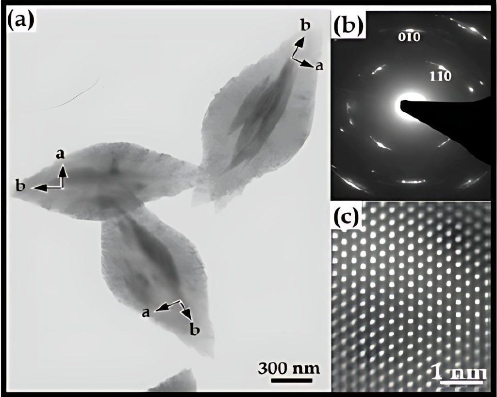
Figure 5: (a) TEM images of the as-grown CuO nanopetals. (b)Associated SAED pattern (c) HRTEM image of the specified area.