Guide
Important equipment for microanalysis techniques include: Optical Microscope (OM), Dual Beam Scanning Electron Microscope (DB-FIB), Scanning Electron Microscope (SEM), and Transmission Electron Microscope (TEM). Today’s article will introduce the principle and application of DB-FIB, focusing on the service capabilities of dual-beam scanning electron microscope (DB-FIB) and cases related to the application of dual-beam scanning electron microscope (DB-FIB) in semiconductor analysis.
What is a Dual Beam Focused Ion Beam/Scanning Electron Microscope?
Dual-beam scanning electron microscope (DB-FIB) integrates focused ion beam and scanning electron beam on one microscope, and then installs accessories such as gas injection system (GIS) and nano manipulator, so as to realize etching, material deposition, micro Instruments with many functions such as nanoprocessing.
Among them, the focused ion beam (FIB) is to accelerate the ion beam generated by the liquid metal gallium (Ga) ion source, and then focus on the surface of the sample to generate signals such as secondary electrons, which are collected and imaged by the detector; or use a strong current ion beam Etch the surface of the sample for micro-nano processing; it can also combine physical sputtering and chemical gas reaction for selective etching or deposition of metal and insulating layers.
Main functions and applications of dual-beam scanning electron microscope (DB-FIB)
Main functions: fixed-point section processing, TEM sample preparation, selective etching or enhanced etching, metal material deposition and insulating layer deposition, etc.
Application fields: At present, the double-beam scanning electron microscope (DB-FIB) is widely used in the research and related product testing of ceramic materials, polymers, metal materials, biology, semiconductors, geology and other fields. In particular, the unique fixed-point transmission sample preparation capability of the dual-beam scanning electron microscope (DB-FIB) makes it an irreplaceable application in semiconductor failure analysis capabilities.
Dual Beam Scanning Electron Microscope (DB-FIB) Service Capabilities
The latest dual-beam scanning electron microscope (DB-FIB) can achieve scanning electron beam imaging resolution below 1 nm, and is more optimized in terms of ion beam performance and automation than the previous generation of dual-beam electron microscope. Dual-beam scanning electron microscope (DB-FIB) is equipped with nanomanipulator, gas injection system (GIS) and energy spectrum EDX, which can meet various basic and advanced semiconductor failure analysis needs.
As a powerful tool for failure analysis of semiconductor physical properties, the dual-beam scanning electron microscope (DB-FIB) can perform fixed-point cross-section processing with nanometer precision, and observe the cross-sectional microscopic morphology and Composition analysis; deposition of different metal materials (tungsten, platinum, etc.) and non-metal materials (carbon, SiO2); TEM ultra-thin slices can also be prepared at fixed points, which can meet the requirements of ultra-high resolution observation at the atomic level.
Dual Beam Scanning Electron Microscope (DB-FIB) Case Sharing
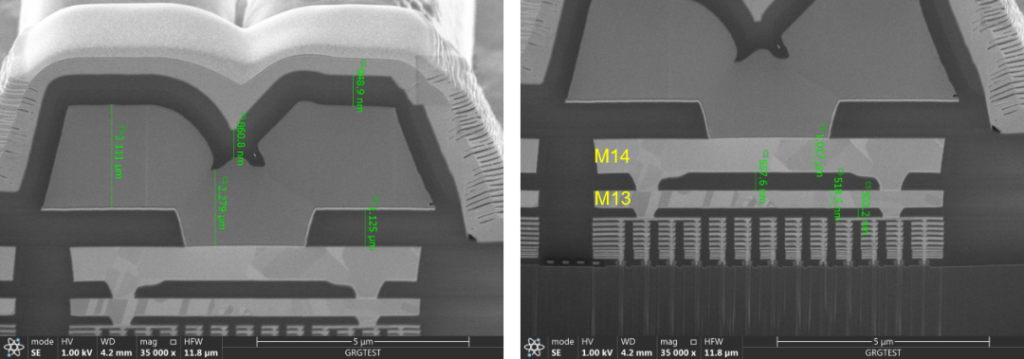
Cross-section analysis of 7nm advanced process chips
Using the fixed-point cross-section processing function of the dual-beam scanning electron microscope (DB-FIB), the cross-sectional morphology analysis and measurement of advanced process chips can be performed, as shown in Figure 2. From M1, M2, all the way to M14 and Top metal layers, the corresponding layer thickness can be clearly observed and measured by dual-beam scanning electron microscope (DB-FIB).
MOS tube failure analysis
When testing the BVDSS project, the Fail die showed ignition and a drop in breakdown voltage, which was initially judged to be a thermal failure. From the back of the chip, use OBIRCH (Optical Beam Induced Resistance Change, laser beam resistance anomaly detection) to determine the hot spot position, and then use a double-beam electron microscope combined with EDX energy spectrum to observe the cross-sectional microscopic appearance of the hot spot position and perform component analysis. The result is shown in Figure 3.
Figure 3 a is a cross-sectional SEM image near the center of the hotspot, where a large area of anomaly (red box) was observed. High-magnification SEM morphology observation and EDX energy spectrum analysis were carried out on the abnormal part, and the results are shown in Figure 3 b) and c). Figure 3 b) is the enlarged image of the red box area in a), and c) is the surface scanning distribution map of some elements in the yellow box area in b). From the results of energy spectrum, it can be seen that the composition of the abnormal point is metal Ni, and at the same time, part of Al melted into the MOS. It is suspected that the photolithography process before the deposition of the Ti layer introduced impurities.
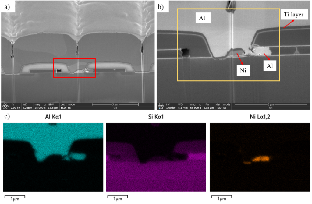
Fig. 3
a) The cross-sectional SEM image of the center of the hotspot, the red box is the anomaly;
b) High magnification image of the anomaly;
c) b)Surface scanning distribution map of Al, Si and Ni elements in the yellow box area in the middle
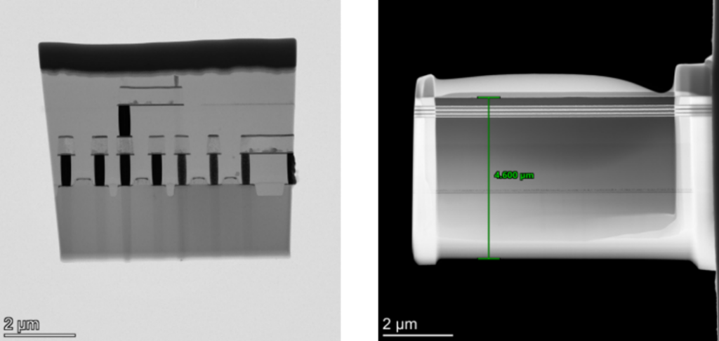
Ultrathin transmission sample preparation
Another most important function of the dual-beam scanning electron microscope (DB-FIB) is to prepare ultra-thin sections of transmission samples. SVA Metrology can currently achieve fixed-point ultra-thin slices below 50 nm, meeting the requirements of TEM observations with atomic resolution.