A scanning electron microscope (SEM) is a very useful large-scale electron microscopic imaging system for failure analysis.

How Scanning Electron Microscopes Work
The working principle of the scanning electron microscope is to use the electron beam emitted by the cathode to be accelerated by the anode, and then focused by a magnetic lens to form a beam of electron beams with a diameter of tens to thousands of Angstroms (Å). Under the deflection of the scanning coil, The electron beam scans point-by-point on the surface of the sample in a certain time and space sequence. When this high-energy electron beam bombards the surface of the sample, it will excite a variety of information. After collection and amplification, various corresponding information can be obtained from the display screen. graphics.
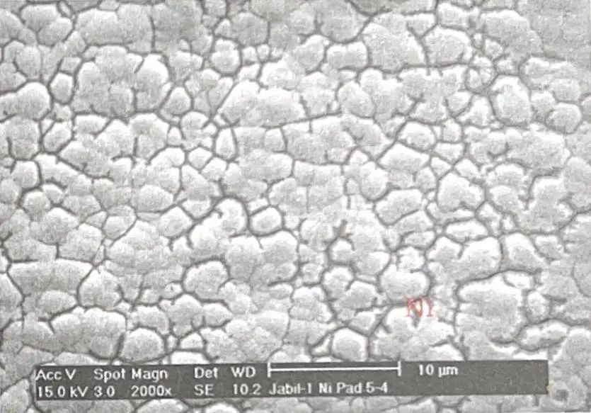
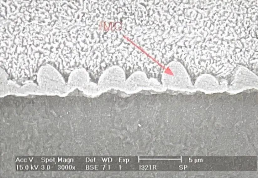
The excited secondary electrons are generated in the range of 5~10nm on the surface of the sample, so the secondary electrons can better reflect the topography of the sample surface, so they are most commonly used for topography observation; while the excited backscattered electrons are generated on the sample surface within 100 nm. In the range of ~1000nm, backscattered electrons with different characteristics are emitted according to the atomic number of the substance, so the backscattered electron image has the ability to distinguish the morphology and atomic number, and the backscattered electron image can reflect the distribution of chemical element components.
The current scanning electron microscope is very powerful, and any fine structure or surface feature can be magnified to hundreds of thousands of times for observation and analysis.

Schematic diagram of scanning electron microscope
Failure Analysis of Solder Joints or Interconnects Using Scanning Electron Microscopy
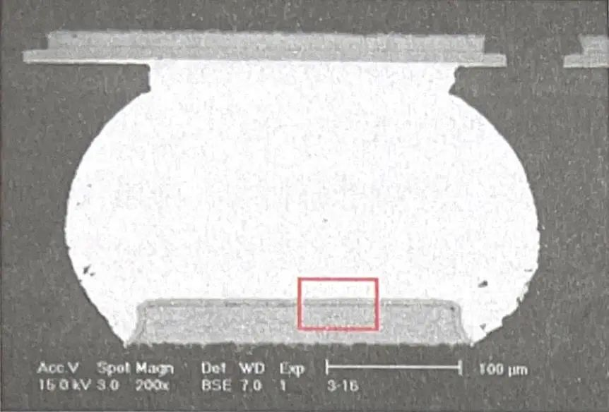
In terms of failure analysis of solder joints or interconnections, SEM is mainly used to analyze the failure mechanism. Specifically, it is used to observe the metallographic structure of solder joints, measure intermetallic compounds, conduct fracture analysis, solderability coating analysis and tin Analytical measurements are required.
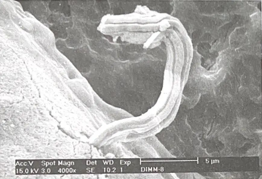
Unlike optical microscopes, scanning electron microscopes form electron images. Therefore, there are only black and white; and the sample of the scanning electron microscope is required to be conductive, and non-conductors and some semiconductors need to be sprayed with gold or carbon, otherwise the charge will accumulate on the surface of the sample and affect the observation of the sample. In addition, the depth of field of the scanning electron microscope image is much larger than that of the optical microscope, and it is an important method for the analysis of metallographic structure, micro fracture and tin whisker.