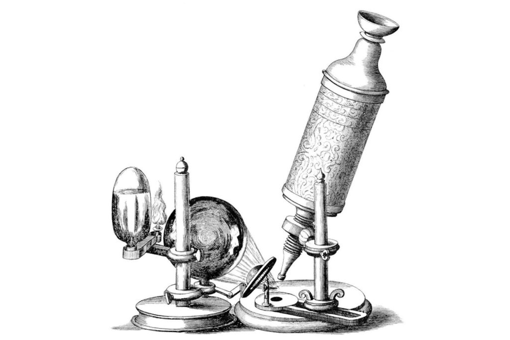
The eye is the first “optical instrument” for human beings to understand the objective world, but its ability is limited. It is generally believed that the resolution of the human eye is 0.1 mm. At the beginning of the 17th century, the optical microscope (Figure 1) appeared, which can magnify small objects to more than a thousand times, and the resolution is more than 500 times higher than that of human eyes. This is also a huge breakthrough for human beings to understand the material world.
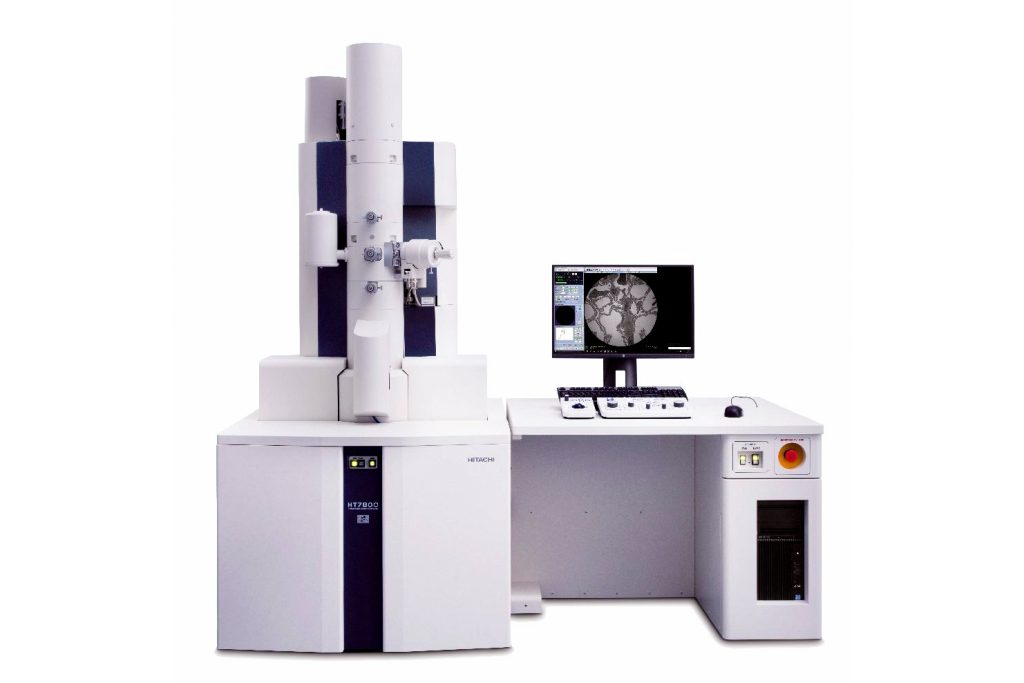
With the continuous development of science and technology, direct observation of atoms has always been the desire of people, and the emergence of electron microscopy has provided the possibility for people to realize this long-cherished wish. With the continuous development and progress of electron microscopy, the resolution of transmission electron microscopy (Figure 2) has reached the sub-angstrom level, and electron microscopy has become an indispensable means of characterization in the field of materials science.
In addition, the combination of electron microscopy and nanoscience, biology, etc., makes the function of electron microscope expand day by day, and it also promotes the rapid development of these fields.
Origin and Development of Transmission Electron Microscopy
Transmission electron microscopy originated in the 1920s and 1930s. In 1924, de Broglie proposed that particles have wave properties. From 1926 to 1927, Davisson, Germer, and Thompson Reid discovered electron diffraction in experiments, thus proving the wave nature of electrons. Therefore, it was thought that electrons could be used instead of visible light to make electron microscopes to overcome the limitation of light wavelength on resolution.
In 1926, German scholar Busch proposed that it is possible to focus electrons by using an axisymmetric magnetic field, which provided a theoretical basis for the production of electron microscopes.
In 1933, Ruska and others made the world’s first transmission electron microscope.
In 1934, the resolution of the electron microscope had reached 500Å, for which Ruska won the 1986 Nobel Prize in Physics.
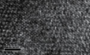
In 1939, Siemens AG of Germany built the world’s first commercial transmission electron microscope (TEM), with a resolution better than 100 Å. Later, Professor Cowley from the Department of Physics of Arizona State University in the United States explained the phase contrast image quantitatively, that is, the so-called high-resolution image (see Figure 3 for the high-resolution TEM image), thus establishing and perfecting the theory of high-resolution electron microscopy And technology.
High-resolution electron microscopy can image the atomic columns in most crystals. At present, high-resolution electron microscopy is a commonly used method in electron microscopy, and its resolution has reached 1-2 Å.
In addition to the wavelength limiting the resolution of the TEM, the aberrations of the TEM, including chromatic aberration, spherical aberration, astigmatism and distortion, also make it difficult for the resolution of the TEM to break through 1 Å. At the end of the 20th century, the spherical aberration corrector was successfully developed. The spherical aberration-corrected electron microscope reduced the influence of the non-localization effect and further improved the resolution of the transmission electron microscope, which has reached the sub-Angstrom level. With the popularity of spherical aberration-corrected electron microscope applications, spherical aberration-corrected electron microscopy is gradually forming and developing.
In addition, with the continuous development of electron microscopy in the past 20 years, scanning transmission electron microscopy (STEM, whose image is shown in Figure 4) has also become a widely used characterization method.
Compared with the traditional high-resolution phase contrast imaging technology, scanning transmission electron microscopy has the advantages of high resolution, sensitivity to chemical components, intuitive and easy-to-interpret images, etc.
Among them, the high-resolution scanning transmission electron microscope can directly obtain the atomic resolution Z-contrast image, combined with the X-ray energy spectrum and electron loss spectrum, it can also obtain the atomic resolution element distribution map and the energy loss spectrum of a single atomic column, so it can Obtain atomic-resolution structural, chemical composition, and electronic structure information in a single experiment.

Applications of Transmission Electron Microscopy
Transmission electron microscopy has the advantages of high resolution and can be used in conjunction with other techniques, and is widely used in the fields of materials science, physics, chemistry and biology.
1. Field of material science
The microstructure of materials plays a decisive role in the physical and chemical properties of materials such as mechanics, optics and electricity. As an important means of material characterization, transmission electron microscopy can not only use the diffraction mode to study the structure of the crystal, but also obtain high-resolution images in real space in the imaging mode, that is, to directly image the atoms in the material and directly observe the microstructure of the material .
Electron microscopy has also played a huge role in promoting the discovery of new materials. D. Shechtman discovered quasicrystals with the help of transmission electron microscopy, redefined crystals, and enriched the connotations of materials science, crystallography, and condensed matter physics. D. Shechtman also won the 2011 Nobel Prize in Chemistry for this.
2. Field of physics
In the field of physics, electron holography can simultaneously provide the amplitude and phase information of electron waves, so that this advanced microscopic analysis method can be widely used in the study of magnetic field and electric field distribution closely related to phase.
At present, electron holography has been applied to measure the electric field distribution of semiconductor multilayer thin film structure devices, the magnetic domain distribution inside magnetic materials and so on.
Zhang Zhe and Zhu Tao from the Institute of Physics, Chinese Academy of Sciences used high-resolution electron microscopy and electron holography to study the microstructure and corresponding barrier layer structure changes of Co-based magnetic tunnel junctions before and after annealing heat treatment. The treatment can obviously improve the interface quality between the barrier layer and the top and bottom electrodes, and improve the structure of the barrier itself.
3. Chemical field
In the field of chemistry, in-situ transmission electron microscopy provides an important method for in-situ observation of gas-phase and liquid-phase chemical reactions due to its ultra-high spatial resolution. In situ transmission electron microscopy is used to further understand the mechanism of chemical reactions and the transformation process of nanomaterials, in order to understand, regulate and design the synthesis of materials from the nature of chemical reactions.
At present, in situ electron microscopy has played an important role in the fields of material synthesis, chemical catalysis, energy applications and life sciences. Transmission electron microscopy can directly observe the morphology and structure of nanoparticles at extremely high magnifications, and is one of the most commonly used characterization methods for nanomaterials.
Du Xiwen from Tianjin University and Houlin L.xin from Brookhaven National Laboratory in the United States observed the morphology changes of Co Ni bimetallic nanoparticles during the oxidation process with in situ transmission electron microscopy. After the fully mixed Co and Ni alloy particles were oxidized, Partial spatial separation of Co and Ni occurs, and this phenomenon is explained theoretically.
4. The field of biology
In the field of biology, X-ray crystallography and nuclear magnetic resonance are often used to study the structure of biological macromolecules, and have been able to determine the position accuracy of proteins to 0.2 nm, but each has its own limitations.
Based on protein crystals, X-ray crystallography often studies the ground state structure of molecules, but is incapable of analyzing the excited and transition states of molecules.
Biomacromolecules often interact and form complexes to play a role in the body, and the crystallization of these complexes is very difficult. Although nuclear magnetic resonance can obtain the structure of molecules in solution and can study the dynamic changes of molecules, it is mainly suitable for studying biological macromolecules with small molecular weights.
In recent years, cryo-electron microscopy has broken through the bottleneck of cryo-imaging and image processing, and has developed into an emerging technology widely used in structural biology today. It can resolve highly complex ultra-large biomolecular structures in a fast, efficient, simple and high-resolution manner, surpassing traditional X-ray crystallography to a large extent.
Shi Yigong’s research group at Tsinghua University extracted endogenous proteins from yeast cells to obtain samples with good properties. Using single-particle cryo-electron microscopy, they analyzed the high-resolution three-dimensional structure of the yeast spliceosome near the atomic level, and elucidated the spliceosome pairing. Mechanism of how pre-messenger RNA performs splicing.
The Development Direction of Transmission Electron Microscopy
Currently, transmission electron microscopy has several important development directions.
First, the improvement of resolution. Resolution has always been the goal and direction of the development of TEM. A new generation of monochromators and spherical aberration correctors has been developed to further improve the energy resolution and spatial resolution of TEM, especially for low-voltage electron microscopes.
Second, the development of in situ transmission electron microscopy technology. In-situ transmission electron microscopy has important applications in the fields of material synthesis, chemical catalysis, life science and energy materials. It can study scientific issues such as the essential mechanism of reactions by observing and controlling the gas-phase and liquid-phase reactions in real time at the atomic scale.
Third, it is more widely used in the study of the structure of biological macromolecules. The wide application of cryo-electron microscopy in the study of the structure of biological macromolecules will promote the continuous development of cryo-electron microscopy. The application of cryo-electron microscopy in the field of biology has attracted more and more attention, and it has become the link and bridge connecting biological macromolecules and cells.
From the birth of the transmission electron microscope to today for more than 80 years, people have solved many scientific problems with the help of the transmission electron microscope. The transmission electron microscope is also constantly developing and progressing, with increasingly comprehensive functions and improved performance. Although there are still some problems and challenges in the development process, I believe that with the joint efforts of all scientific researchers, the problems will eventually be solved. Various technologies of the transmission electron microscope It will also develop and break through further.