Definition:
An electron microscope in which a beam of electrons reflected by a sample makes an image.
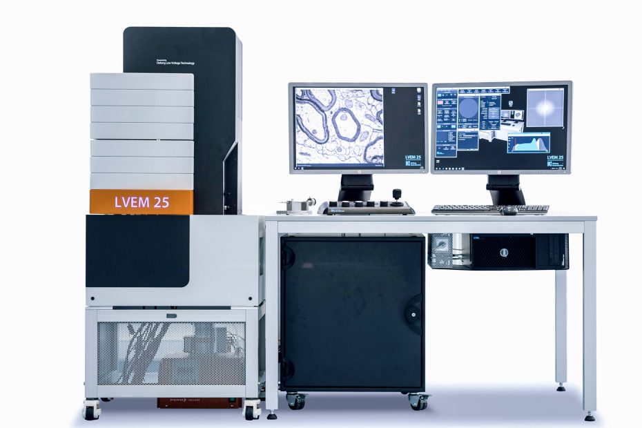
Low-voltage scanning electron microscope technical features:
Low-voltage scanning electron microscopy (LVSEM), defined as operating in the energy range below 5 keV, has become perhaps the most important single mode of operation for SEMs.
This is due to the advantages of LVSEM in surface imaging, observation of poorly conducting and insulating materials and high spatial resolution X-ray microanalysis. These benefits are all due to the rapid decrease of the electron range R due to the reduction of the incident beam energy E0, since R~k.E01.66. The reduction in beam penetration has important consequences.
First, the sample volume sampled by the beam shrinks dramatically (approximately E05 change), so the beam-generated information is confined to the sample surface.
Second, the yield ↑ of secondary electrons increases from a typical value of 0.1 at 20 keV to a value that may exceed 1.0 at 1 keV. The yield ↑ of backscattered electrons also varies, albeit less dramatically, tending to rise for low atomic number (Z<30) elements and fail for high atomic number elements.
Third, due to the large increase in the secondary electron signal, the total emitted electron yield can reach unity at certain energies. When this happens, no net charge is deposited in the sample, so even insulators can be observed without the problem of charge accumulation.
LVSEM operation also has some potential disadvantages, the image is highly sensitive to the state of the sample surface, so contamination can be a major concern, and the rapid reduction of the interaction volume means that the incident beam dose is concentrated. As a result, beam-induced radiation damage is enhanced even though the size of the region where it occurs is reduced.
It is difficult at low beam energies to match the electron-optical performance that can be achieved at higher voltages.
This is because the brightness of any emitter scales linearly with beam energy, so the performance of all electron sources degrades significantly at low voltages.
In addition, the combination of chromatic aberration of the probe-forming lens and energy spread of the beam creates a substantial “skirt” around the probe, which increases the diameter of the probe, destroys resolution, and reduces image contrast.
At the lowest energies (i.e., below 250eV), the relatively large electron wavelengths further reduce resolution due to diffraction, and the depth of field of the instrument is also reduced.
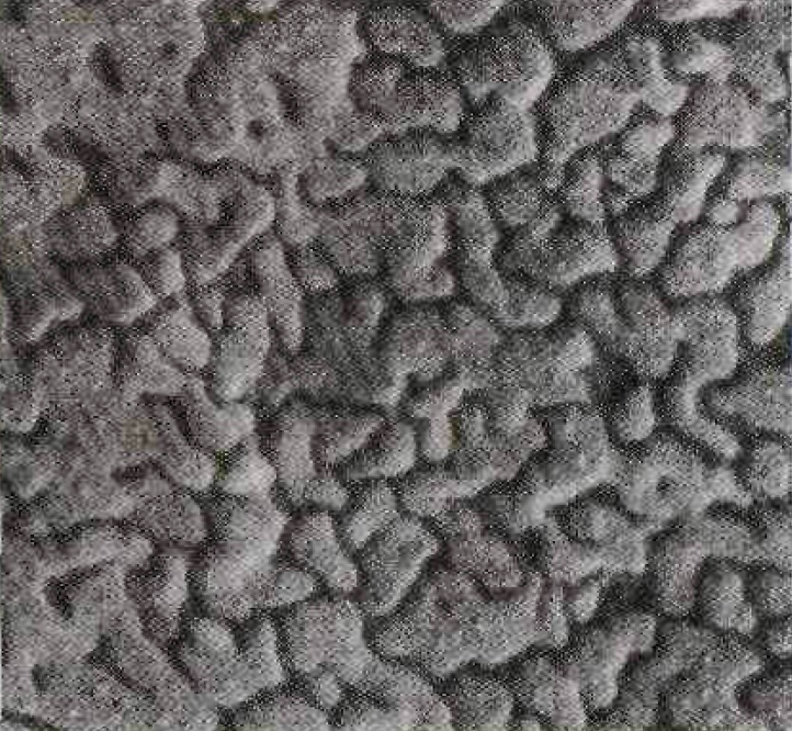
Despite these issues with current LVSEMs, a resolution of around 2nm at 1 keV can be achieved with conventional optics when using a field emission gun.
This level of performance can be maintained at energies below 100eV if delayed field optics are employed (Figure 1).
X-ray microanalysis in the low voltage region (E0 < 5 keV) offers particular advantages compared to conventional beam energy ranges (15 < E0 < 30 keV), but it is also limited by potentially severe limitations. On a positive note, the reduction in the electronic range at low voltages is complemented by a more steep decline in the X-ray excitation range Rx~(E01.67-Ec1.67). The shallow X-ray range results from the operation of many elements close to the critical excitation potential E, and results in sampling quality in the femtosecond range and lateral resolution below 50nm. Due to the low overvoltage (U=E0/Ec) and due to the very shallow x-ray production, typically 100nm or less, the matrix corrections due to electron scattering and delay and x-ray absorption tend towards values close to unity, reducing principle-related errors.
On the negative side, low beam energies severely limit the accessible atomic shells of middle and high atomic number elements, and even for these shells, low fluorescence yields and low overvoltages lead to low spectral peaks/background (P /B). The combined effect of these effects is to limit access to trace concentration levels (arbitrarily defined as C < 0.01), and in some particularly difficult cases, it is even difficult to detect trace components (0.01 < C < 0.1). Low-voltage microscopy is often effectively applied as a means of avoiding or at least reducing charging effects in images of uncoated insulators.
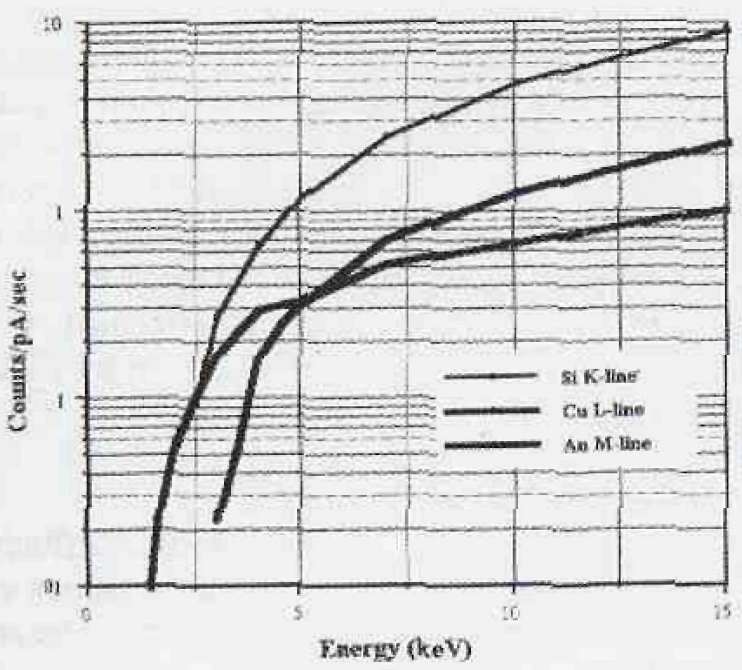
While stable imaging can often be achieved under these conditions, special care must be taken when performing X-ray microscopic analysis under these conditions. Since the overvoltage is so low, even slight charging can significantly change the efficiency of X-ray generation, which is exponentially related to the overvoltage: I-(U-1)n, where 15 < n < 1.7 {Fig. 2). To test for charging, analysts can use EDS spectroscopy to monitor the Duane-Hunt-limit of x-ray bremsstrahlung, which is equal to the energy of the electron beam hitting the sample. However, charging is usually a dynamic process, so it must be monitored with sufficient time sampling. Otherwise, the relative peak heights observed for elemental mixtures can be very misleading.
Low Voltage Scanning Electron Microscope Market Outlook:
According to GIR (Global Info Research), in terms of revenue, the global low-voltage electron microscope (LVEM) revenue in 2021 will be approximately US$1,280 million, and it is expected to reach US$1,827.2 million in 2028, with a CAGR of 5.2 between 2022 and 2028 %.