1. What is a high-resolution transmission electron microscope
High-resolution transmission electron microscopy (referred to as HRTEM or HREM) is phase contrast (the contrast of high-resolution electron microscopy images is formed by the phase difference between the synthesized projected wave and diffracted wave, called phase contrast.) Microscopy, which can obtain images of the atomic arrangement of most crystalline materials.
2. History of high-resolution transmission electron microscopy
High-resolution transmission electron microscopy began in the 1950s. In 1956, J.W.Menter directly observed parallel stripes of copper phthalocyanine with a spacing of 12 Å with a transmission electron microscope at a resolution of 8 Å, which opened the subsequent high-resolution electron microscopy. the door of art.
In the early 1970s, Sumio Iijima took a phase contrast image of Ti2Nb10O29 with a TEM with a resolution of 3.5Å in 1971, and directly observed the projection of the atomic group along the direction of the incident electron beam. At the same time, important progress has been made in the study of explaining high-resolution imaging theory and analysis technology.
In the 1970s and 1980s, electron microscopy technology was continuously improved, and the resolution was greatly improved. Generally, large-scale TEMs can guarantee a lattice resolution of 1.44Å and a point resolution of 2-3Å. HRTEM can not only observe the lattice fringe image reflecting the spacing of crystal planes but also observe the structural image reflecting the arrangement of atoms or atomic groups in the crystal structure.
Recently, the team of Professor David A. Muller of Cornell University in the United States has achieved a spatial resolution of 0.39 Å under low electron beam energy imaging conditions by using stacked imaging technology and self-developed electron microscope pixel array detectors.
3. High-resolution transmission electron microscope imaging process
The transmission electron microscopes currently produced are generally capable of HRTEM, and these transmission electron microscopes are divided into two categories: high-resolution and analytical.
The high-resolution TEM is equipped with a high-resolution objective lens pole piece and diaphragm combination, which makes the sample stage tilt angle very small, thereby obtaining a small spherical aberration coefficient of the objective lens; while the analytical TEM needs a larger lens for various analysis. The tilt angle of the sample stage, so the pole shoe of the objective lens is used differently from the high-resolution type, which affects the resolution.
In general, a 200 keV high-resolution TEM has a resolution of 1.9 Å, while a 200 keV analytical TEM has a resolution of 2.3 Å. But this does not affect the analytical TEM to take high-resolution images.

As shown in Fig.1, it is a schematic diagram of the optical path of the high-resolution electron microscopy imaging process. When an electron beam with a certain wavelength (λ) is incident on a crystal with an interplanar spacing of d, when the Bragg condition (2dsinθ=λ) is satisfied, at a specific A diffracted wave is produced at the angle (2θ).
The diffracted waves converge into one point on the back focal plane of the objective lens to form diffraction spots (in an electron microscope, the regular diffraction spots formed on the back focal plane are projected onto the fluorescent screen, which is the so-called electron diffraction pattern.).
When the diffracted wave on the back focal plane continues to move forward, the diffracted wave synthesizes to form an enlarged image (electron microscopic image) on the image plane. When a large objective lens diaphragm is inserted on the back focal plane, more than two Wave interference imaging is called high-resolution electron microscopy, and the observed image is called high-resolution electron microscopy (high-resolution microscopy).
4. Interpretation of high-resolution electron micrographs
As mentioned above, high-resolution electron microscopy is like letting the transmitted beam and several diffracted beams of the rear focal plane of the objective lens pass through the objective lens diaphragm, and a phase contrast microscopic image is formed due to their phase coherence.
Due to the different numbers of diffracted beams participating in imaging, high-resolution images with different names are obtained.
Due to different diffraction conditions and sample thicknesses, high-resolution electron microscopic images with different structural information can be divided into five categories for illustration: lattice fringes, one-dimensional structure images, and two-dimensional lattice images (images at the unit cell scale), two-dimensional structure images (atomic scale image: crystal structure image), special image.
Lattice fringes: If a transmitted beam and a diffracted beam on the back focal plane are selected by the objective lens diaphragm to interfere with each other, a fringe pattern with periodic intensity changes in one dimension is obtained (as shown by the black triangle in Fig.2 (f)) , which is that the lattice fringe is different from the lattice image and the structure image, and it does not require the electron beam to be exactly parallel to the lattice plane.
In fact, in the observation of crystallites and precipitates, lattice fringes are often obtained by interference of projected waves and diffracted waves.
If electron diffraction patterns with micro crystals and other substances are photographed, Debye rings will appear, as shown in (a) of Fig.2.
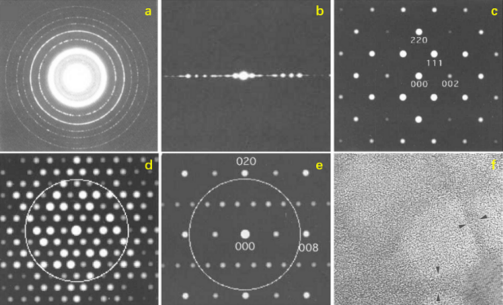
One-dimensional structure image: If the sample has a certain tilt so that the electron beam is incident parallel to a certain crystal plane family of the crystal, it can satisfy the one-dimensional diffraction pattern shown in Fig.2(b) (symmetrically distributed with respect to the transmission spot Diffraction patterns).
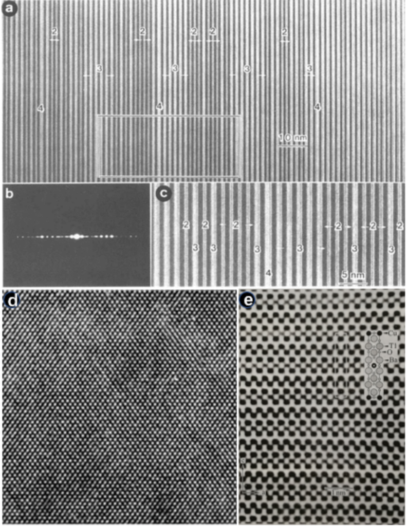
Under this diffraction pattern, the high-resolution image taken under the best focusing condition is different from the lattice fringe, and the one-dimensional structure image contains the information of the crystal structure, that is, the obtained one-dimensional structure image, as shown in Fig.3(a ) shows the high-resolution one-dimensional structure image of Bi-based superconducting oxides.
Two-dimensional lattice image: If the electron beam is incident parallel to a certain crystal zone axis, a two-dimensional diffraction pattern can be obtained (as shown in Fig.2(c), which is a two-dimensional symmetrical distribution relative to the central transmission spot). For such an electron diffraction pattern.
Near the transmission spot, a diffracted wave reflecting the crystal unit cell appears. In the two-dimensional image generated by the interference of the diffracted wave and the transmitted wave, a two-dimensional lattice image showing the unit cell can be observed, although this image contains information on the unit cell scale.
However, it does not contain information on the atomic scale (arrangement of atoms in a unit cell), that is, the two-dimensional lattice image is the two-dimensional lattice image of single-crystal silicon as shown in Fig.3(d).
Two-dimensional structural image: Obtain the diffraction pattern shown in Fig.2(d). When using such a diffraction pattern to observe a high-resolution electron microscopic image, the more diffraction waves that participate in the imaging, the more information contained in the high-resolution image. more and more.
As shown in Fig.3(e), it is a high-resolution two-dimensional structure image of Tl2Ba2CuO6 superconducting oxide. However, the diffraction on the high-wavenumber side, where the resolution limit of the electron microscope is higher, cannot participate in the imaging of correct structural information and becomes the background.
Therefore, within the range allowed by the resolution. By imaging with as many diffracted waves as possible, an image containing correct information about the arrangement of atoms in the unit cell can be obtained. Structural images can only be observed in the thin regions excited by the waves participating in the imaging in proportion to the thickness of the sample.
Special image: On the diffraction pattern of the back focal plane, inserting a diaphragm and only selecting a specific wave for imaging can observe an image with a specific structural information contrast. A typical example of it is the ordered structure image. The corresponding electron diffraction pattern is shown in Fig.2(e) as the electron diffraction pattern of Au, Cd ordered alloy.
The ordered structure is based on the face-centered cubic structure, in which Cd atoms are arranged in an orderly manner. In addition to the strong basic lattice reflections of indices (020) and (008), the electron diffraction pattern in Fig.2(e) appears weak Ordered lattice reflection, using the objective lens diaphragm to get rid of the basic lattice reflection, when using transmitted wave and ordered lattice reflection imaging, only Cd atoms appear as bright or dark spots as shown in high-resolution image Fig.4
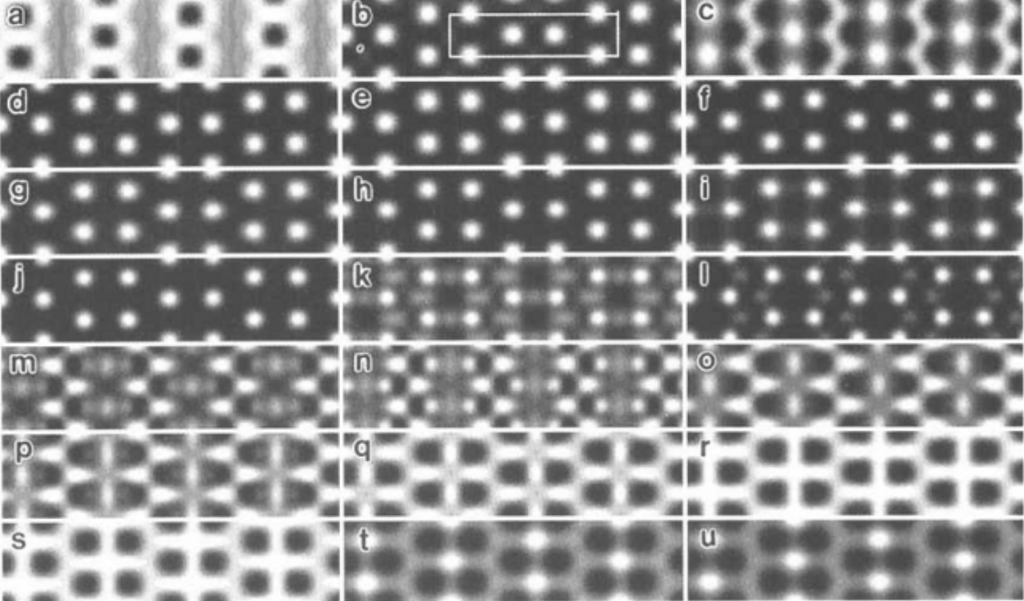
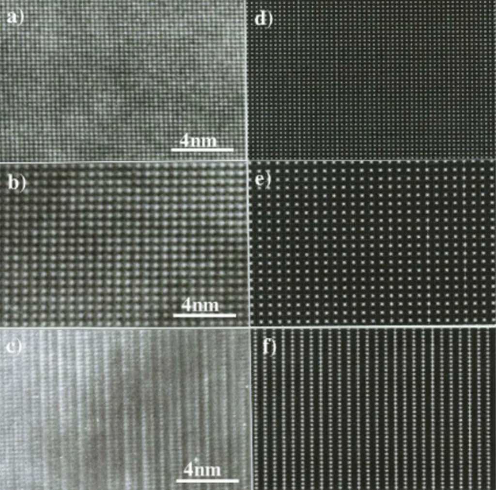
As shown in Fig.4, near the optimal high-resolution under-focus amount, as the thickness of the sample changes, the displayed high-resolution images are also different.
Therefore, when we get a high-resolution image, we cannot simply say what crystal structure this high-resolution image is, but must first do computer simulation calculations, and calculate the structure of the material under study under different thicknesses and different under-focus amounts. A high-resolution image of the substance.
A series of high-resolution images calculated by the computer are compared with the high-resolution images obtained by the experiment, so as to determine the high-resolution images obtained by the experiment. The computer simulation image shown in Fig.5 is compared with the high-resolution image obtained by the experiment.