When we characterize the morphology of a catalyst or sample, we usually use transmission electron microscopy. At this time, we often use the term, contrast.
Contrast, the popular explanation is the difference in color depth between different nanoparticles in the transmission electron microscope image.
Contrast refers to the difference in lightness and darkness between different regions on an image, and it is precisely because of contrast that we can see various specific images.
Imaging contrast is another key issue of optical microscopes. Some objects observed by the microscope, such as biological specimens, have very little brightness difference between the details. In addition, the design and manufacturing errors of the microscope optical system further reduce the imaging contrast and make it difficult to distinguish. At this time, The inability to see the details of the object is not because the total magnification is too low, nor is the numerical aperture of the objective lens too small, but because the contrast of the image surface is too low.
How is contrast defined? How did it come about? How do we use the concept of contrast? Today we mainly summarize these three issues.
#1 Source of contrast?
The history of observation of thin-film crystal samples by transmission electron microscopy can be traced back to the 1950s. Hirsh and Bollman et al. applied this technology to imaging by using electron diffraction effects, and obtained a lot of information related to the crystal structure of materials from electron microscopy.
The so-called contrast specifically refers to the difference in electron beam intensity between two adjacent parts of the sample. Before talking about contrast, we must first mention how the transmission electron image is generated.
1.1 How are transmission electron images produced?
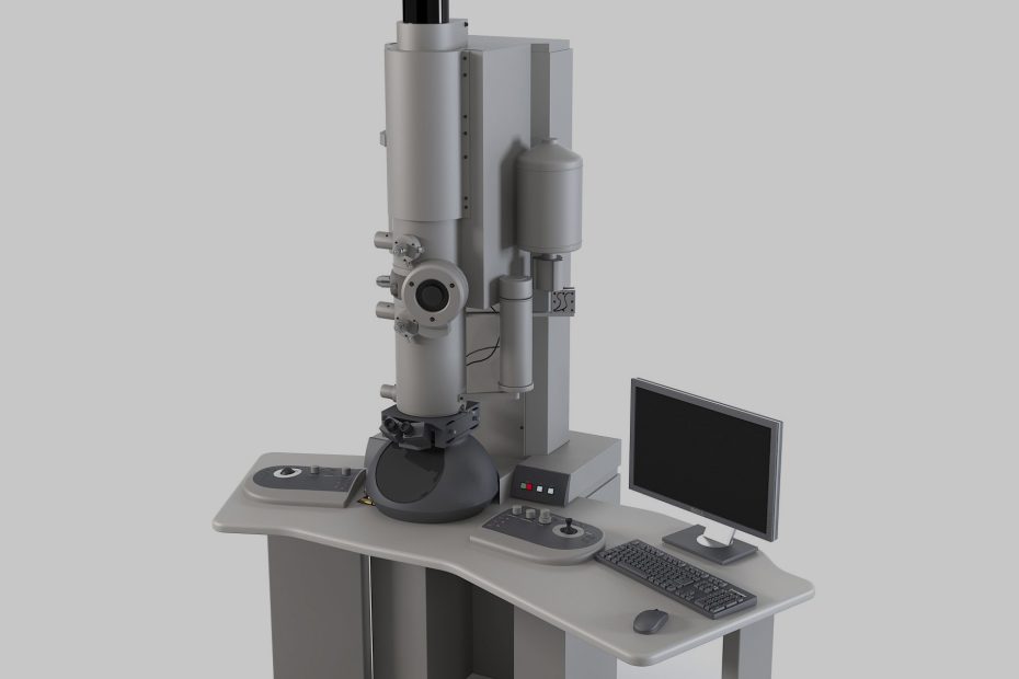
Figure 1 shows the appearance of a common TEM device. The basic process of imaging is this:
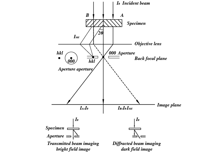
Electrons are emitted from the electron gun, accelerated in the vacuum acceleration tube, focused by the lens in the illumination system and hit the sample, the electron beam interacts with the sample, is diffracted, and the electrons carrying the sample information are captured by the imaging system and amplified imaging.
The imaging here is mainly due to Abbe’s principle. Abbe’s imaging principle is actually the second diffraction theory.
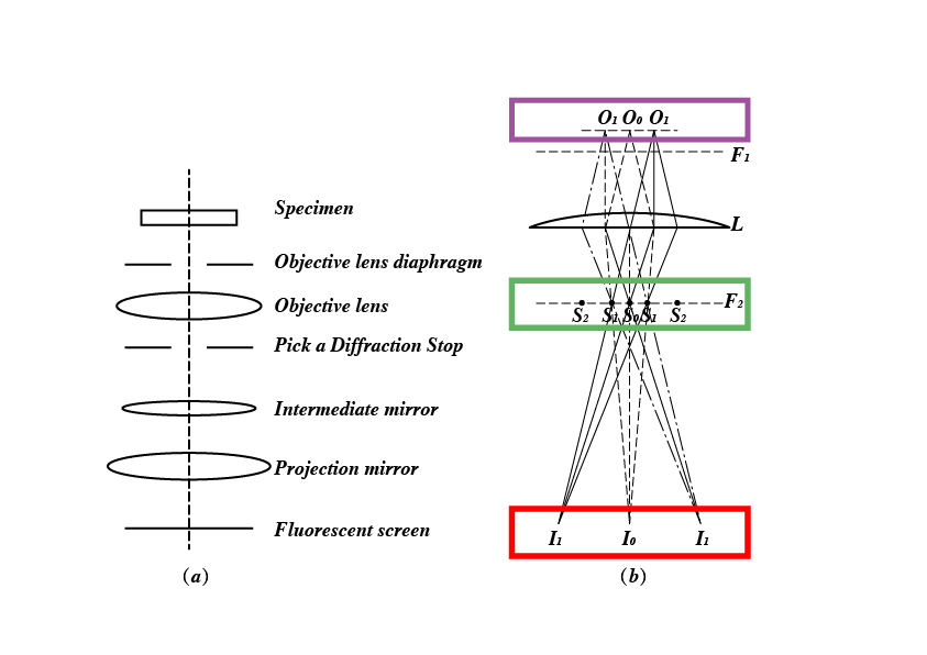
Electron beam diffraction occurs when a parallel beam of light passes through a periodic structure. As shown in Figure 2, Abbe regarded the lens imaging process as two steps.
The first step is to form a series of diffraction spots after the object image passes through the lens, and the phase information of the object is displayed through the diffraction spectra of all levels. The second step is to re-interfere and superimpose the diffraction spectra at all levels to re-form the phase of the object.
A similar process can be achieved by using an electron beam to pass through a thin film sample by adding an intermediate mirror and a projection mirror. When the current of the intermediate mirror is changed to move the object plane from the objective mirror plane to the rear focal plane of the objective lens, the diffraction spectrum can be obtained. If it is moved to If the mirror plane of the object is obtained, the image of the object can be obtained.
Therefore, using a transmission electron microscope, we can not only observe the diffraction spectrum, but also directly see the image of the object.
#2 Generation of contrast
The formation of the transmitted electron image depends on the interaction between the incident electron beam and the material. When the electrons pass through the sample surface, the intensity of the transmitted electron beam will change due to the different effects on the electrons in different regions of the sample, so the intensity transmitted to the fluorescent screen will change. Inhomogeneity is reflected in the difference in brightness, and the electronic image with uneven intensity is the contrast image.
The contrast of electron microscopic images mainly includes mass-thickness contrast, diffraction contrast, phase contrast, and Z contrast.
Mass-thickness contrast: caused by differences in the average atomic number or thickness of different regions in the sample.
Diffraction Contrast: Caused by differences in the crystallographic features of different regions within a sample. It can also be considered as the contrast caused by the difference in the degree to which different parts of the crystal film meet the Bragg diffraction conditions.
Phase contrast: It is caused by the phase difference of the electronic wave modulated by the sample.
Z contrast: It is related to the average atomic number of the sample micro-region.
caused by differences
Definition: Also known as lining value, it describes the degree of a certain value or a certain parameter, and is the ratio of its value to its base.
Such as anomalous lining value (geology): the ratio of the average content of elements in the anomaly to the background value. It is a measure of abnormal clarity, so it is also called abnormal clarity.
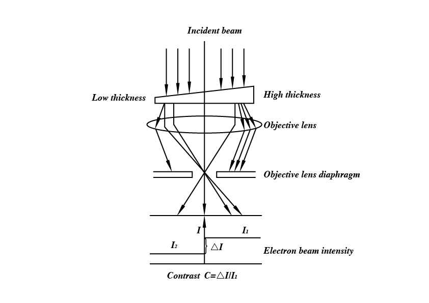
2.1 Mass-thickness contrast
The so-called mass-thickness contrast refers to the difference in contrast caused by the difference in thickness and mass of different regions on the surface of the sample. Since each part of the sample has a different ability to scatter electrons, the number of transmitted electrons passing through the objective lens is also different, so the intensity of the electron beam will vary. Scattering is strong, and the image of the area with few transmitted electrons is dark, otherwise, the image is bright.
2.2 Diffraction contrast
If the thickness of each region of a sample is basically the same, and the average atomic number is not much different, their scattering and absorption of electrons are roughly the same, so satisfactory image contrast cannot be obtained by using the mass-thickness contrast, and the image can be obtained by using the diffraction contrast.
Diffraction contrast refers to the contrast caused by the difference in diffraction intensity formed by crystal samples satisfying the Bragg equation to different degrees and structural amplitudes.
For example, there are two crystals A and B in the sample, adjust the direction of the incident beam, A does not meet the Bragg diffraction conditions, and no diffraction occurs when the electron beam passes through, so the intensity of the transmitted beam of A sample is equal to the intensity of the incident beam; if B satisfies the diffraction conditions, then B The intensity of the transmitted beam of the sample will be less than the intensity of the incident beam, so on the fluorescent screen, A will be brighter than B, which is a bright field image.
However, if the lens grating is adjusted so that the electron beam corresponding to the diffraction point passes through and the transmitted beam is blocked, then B will be brighter than A, and a dark field image will be formed.
Under dark field imaging conditions, the brightness of the sample image is directly equal to the diffraction intensity of the electron beam corresponding to the direction of the grating, so it can reflect the crystallographic characteristics of different parts of the sample.
2.3 Phase contrast
The electron beam propagates through a very thin sample. The Coulomb field generated by the nucleus and the electrons outside the nucleus in the sample will cause the phase of the electron wave to fluctuate. If this phase change can be converted into image contrast, it is called phase contrast. The sample is very thin, less than 10nm, the main phase contrast. When the sample is relatively thick, the mass-thickness contrast and diffraction contrast are mainly formed. A high-resolution image is a phase contrast image.
3 Application of contrast concept
After understanding the source of contrast in TEM imaging, it can be applied in at least the following angles.
3.1 The transmission electron microscope can be used in a well-founded way to optimize the samples we see
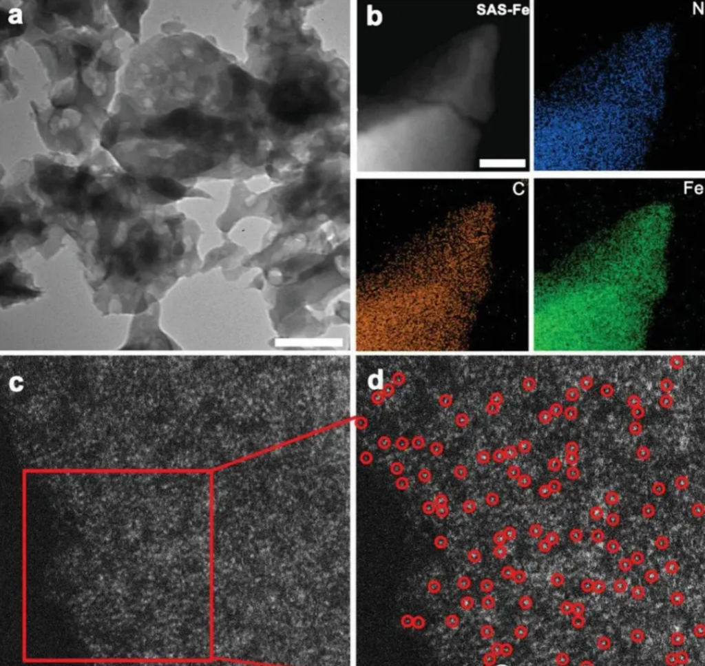
such as the use of bright field images and dark field images, so that our target samples can be displayed more clearly, and dark field images combined with mapping can be better-displayed Sample size and distribution of nanoparticles in the catalyst.
For example, the common form of the image below in the article is usually combined with a low-resolution transmission image, plus a dark field image and mapping, and the single-atom iron image marked in the spherical aberration electron microscope. Among them, iron has a difference in contrast due to the difference in atomic number with other surrounding elements. Generally, the higher the atomic number, the more serious the scattering of electrons, and the darker the brightness of the bright field image.
3.2 Judge some interferences.
For example, for some samples adsorbed by organic matter, since the organic matter is mainly composed of carbon and hydrogen elements, the difference in contrast with other elements in the sample may not be very large, and it is easy to be decomposed under the irradiation of high-energy electron beams, so when you see some strange images on the fluorescent screen Based on this, it can be judged whether it is caused by sample contamination, rather than the contrast caused by the sample itself.