1. Summary of various signals and contrast
Secondary electron imaging (SE) uses the electron imaging of the outer layer of the sample bombarded by incident electrons. The energy is low, and it can only characterize the surface of the sample, and the resolution is relatively high.
- Mainly shape information, with composition contrast
- High resolution
- Energy less than 50eV
Backscattered electrons (BSE) are incident electrons scattered by the sample and then imaged, with high energy close to the incident electrons. It can reflect the deep information inside the sample, and the resolution is relatively low.
- The atomic number is the main factor, with shape contrast
- Energy close to the original electron beam
- There are low angle, high angle, and top angle, and different types carry different contrast
Similar to backscattered electron detectors, STEM detectors are generally made of semiconductor materials and divided into several pieces.
One of them is located directly below the sample and is mainly used to receive the transmitted electrons passing through the sample, which is the so-called bright field mode;
the other is located around the bright field detector to receive the scattered transmitted electrons, which is the so-called dark field mode model.
- Mass-thickness contrast
- Diffraction contrast
- Composition contrast
The relationship between various electronic signals, current signals, electromagnetic wave radiation signals, and various contrasts involved in the scanning electron microscope, the following is a summary of common electronic signals and contrasts, as shown in Figure 1 and Table 1.
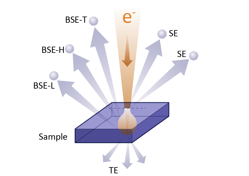
| Type | Classification | Primary contrast | Secondary contrast | Resolution |
| Secondary electronics SE | SE1 | Morphology | Composition, channel | High |
| SE2、SE3、SE4 | channels | Low | ||
| Backscattered electronsBSE | High Angle | Composition | Morphology, Channels | Higher |
| Low angle | Composition | Low | ||
| Transmission electrons TE | Low angle | Mass-thickness | Very high | |
| Medium | Diffraction | Very high | ||
| High angle | Atomic number | Very high |
2. Charging effect
There is also an undesirable phenomenon in the scanning electron microscope, such as the charging effect, which can also form some special contrast. However, in the process of SEM observation, we need to avoid it as much as possible.
2.1. Charge Formation
According to the scanning electron microscope principle introduced above, the electron beam continuously bombards the sample.
According to Figure 2, only when the energy of the original electron beam is v1 and v2, is the secondary electron yield δ is 1, that is, the incident electron and the secondary electron The number of electrons is equal, the sample does not increase or decrease electrons, and no absorption current is formed.
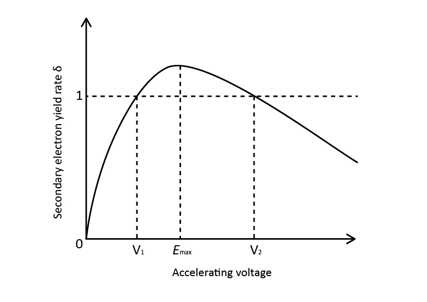
As long as the initial electron beam does not satisfy this condition, an absorption current must be formed to satisfy the charge balance, i0=ib+is+ia. To achieve charge balance, the sample needs to have good conductivity. For conductors, observation is no problem.
However, for samples that are non-conductive, poorly conductive, or poorly grounded, the excess charge cannot be conducted away and will accumulate on the surface of the sample, generating an electrostatic field that interferes with the emission of the incident electron beam and secondary electrons. electric effect.
The charging effect will have a series of effects on the image, such as:
① Abnormal contrast: The secondary electron emission is affected by irregularities, causing part of the image to be abnormally bright and partly dark;
② Image distortion: due to the electrostatic field effect generated by charging, the incident electron beam is deflected irregularly, resulting in image distortion or stage difference;
③ Image drift: Due to the action of the electrostatic field, the incident electron beam is deflected in a certain direction to form image drift;
④ Bright spots and bright lines: Irregular discharges often occur in samples with spots, resulting in irregular bright spots and bright lines in the image;
⑤ The image is “very flat” and has no three-dimensional effect: usually, the scanning speed is slow, and the dwell time of each pixel is longer, which causes charge accumulation, the image looks flat, and completely loses the three-dimensional effect.
Figure 3 is a typical charging effect.
2.2. Elimination of charge
The generation of charge has a great impact on the observation of the scanning electron microscope, so only by eliminating or reducing the charging effect can normal scanning electron microscope observation be carried out.
There are many ways to eliminate and reduce the charge, and here are the commonly used methods.
First of all, in the sample preparation process, attention should be paid to reducing the charge:
1) Reduce the size of the sample and reduce the contact resistance as much as possible: this can increase the conductivity of the sample.
2) Coating treatment: Coating a layer of conductive film on the sample to improve its conductivity, which is also the most used method.
Commonly used coatings include evaporation and ion sputtering. Commonly used conductive films are generally gold au and carbon. If better effects are sought, platinum pt, chrome cr, iridium ir, etc. can also be used.
Plating a conductive film can not only effectively improve the conductivity, but also increase the secondary electron excitation rate, and the current film thickness is relatively easy to control, and it will not affect the sample morphology within a certain magnification. However, the coating also has its disadvantages.
After the coating, there will be a film covering, which will affect the real shape of the sample. In severe cases, it will also produce false images. For some ultra-high resolution observations or the measurement of some details (such as pores, fibers) and eds, best analysis has a greater impact.
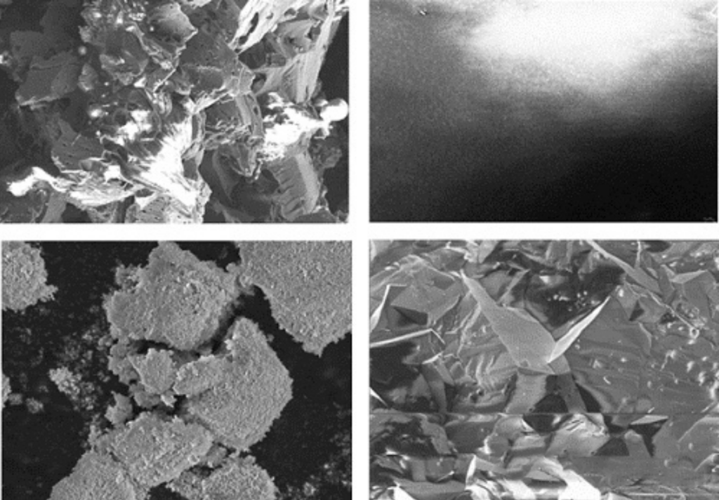
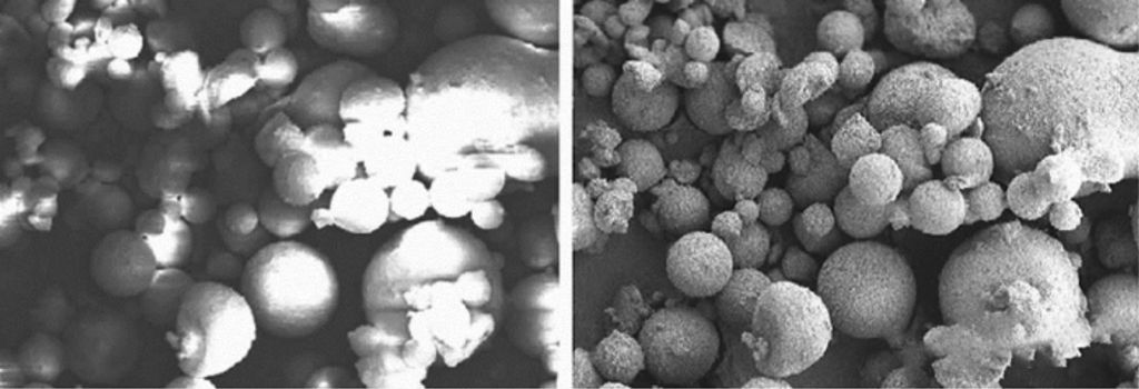
As shown in Figure 4, after the graphite is coated with pt film, false images are produced; as shown in Figure 5, after the fiber is plated with gold, the microscopic becomes thicker and the pores become smaller.
In addition to sample preparation, it is also necessary to find suitable electron microscope working conditions as much as possible to eliminate or weaken the influence of charging:
3) Reduce the beam current: reduce the intensity of the incident electron beam, which can reduce the accumulation of charges.
4) Reduce the magnification: use low magnification observation as much as possible, because the larger the magnification, the smaller the scanning range and the faster the charge accumulation.
5) Increase the scanning speed: The electron beam stays in the same area for a long time, which is easy to cause charge accumulation; at this time, the scanning speed of the electron beam can be increased, and the time spent in different areas can be shortened to reduce the charge.
6) Change the image acquisition strategy: After the scanning speed becomes faster, the signal-to-noise ratio of the image will be greatly reduced. At this time, the use of line accumulation or frame superposition averaging can reduce the charging effect and improve the signal-to-noise ratio.
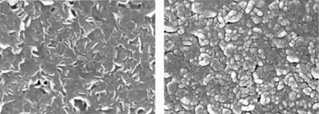
Line accumulation has a good suppression effect on slight charging; frame superposition has a good suppression effect on high noise generated by fast scanning, but the image must not drift, otherwise ghosting will cause image blur. As shown in Figure 6, the sample is a polymer sphere.
When the scanning speed is slow, the sample is easily damaged and deformed. However, with the acquisition method of fast scanning and line accumulation at the same time, the sample is intact and the image still has a good signal-to-noise ratio.
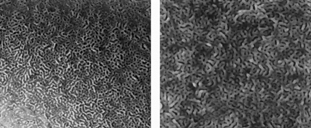
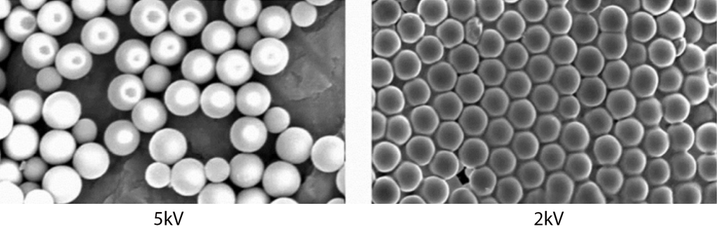
7) Reduce the voltage: Reducing the energy of the incident electron beam (to within v2) can also effectively reduce the charging effect. As shown in Figure 7, the sample is a polystyrene ball, and the charging phenomenon is obvious when the accelerating voltage is 5kV, and the charging is basically eliminated when the acceleration voltage drops to 2kV. However, with the reduction of the accelerating voltage, it will also bring the side effect of the reduction of resolution.
8) Observe with a secondary electron detector or a backscattered electron detector, not in the lens barrel: when a large amount of charge is generated, a large number of secondary electrons will be pushed upwards, but the secondary electrons in the lens barrel receive Too much electronic signal will generate a charge, especially in the immersion mode.
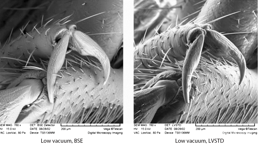
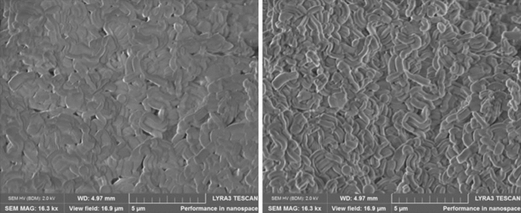
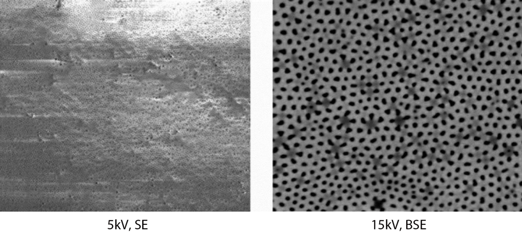
At this time, the detector outside the pole piece is used, and the electronic signal received by it is relatively small, which can weaken the charging effect, as shown in Figure 8; The energy of the electrons is high, and its output and emission direction are much less affected by the charge than the secondary electrons, so observation with the base image can also effectively weaken the charge effect, as shown in Figure 9, the alumina template is in the secondary electron and Contrast under backscattered images.
9) Tilt the sample: Tilt the sample at a certain angle, which can increase the output of secondary electrons of the sample, thereby weakening the charging effect.
In addition, electron microscope manufacturers are also developing new technologies to reduce or eliminate charging, the most common being low vacuum technology.
Low vacuum technology is a very effective means to eliminate the charge of the sample, but the electron microscope itself needs to be equipped with this technology.
10) Low vacuum mode: In low vacuum mode, ionized ions or gas molecules can be used to neutralize the charge, so that the charge effect can be eliminated without coating or harsh electron microscope conditions.
However, under low vacuum conditions, the original electron beam will be scattered by gas molecules, so the resolution, signal-to-noise ratio, and contrast will all be reduced to a certain extent.
As shown in Figure 10, the observation of the uncharged effect of secondary electrons and backscattered electrons can be realized without coating the conductive film on biological samples.