
Electron microscopes are extremely versatile instruments that can provide various types of information according to the user’s requirements. In this article, we will describe the different types of electrons produced in an SEM, how to detect them, and the type of information they can provide.
As the name implies, an electron microscope uses a beam of electrons to make images. In Figure 1, it is possible to see the various products that may arise due to the interaction between electrons and matter. All of these different types of signals convey different beneficial information about the sample, and the microscope operator can choose which ones to capture.
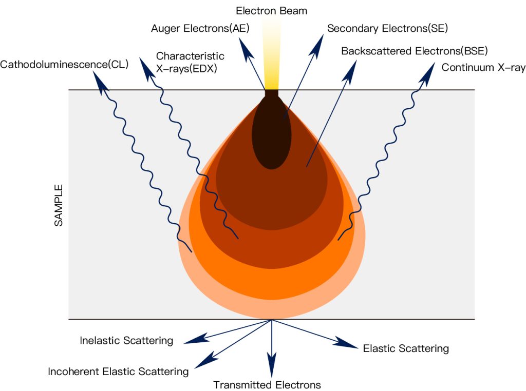
For example, in a transmission electron microscope (TEM), as the name implies, signals such as transmitted electrons are detected that provide information about the internal structure of the sample.
In the case of scanning electron microscopy (SEM), two types of signals are typically detected; backscattered electrons (BSE) and secondary electrons (SE).
Backscattered Electron (BSE) Imaging
Backscattered electrons (BSE)
Backscattered electrons refer to a part of incident electrons reflected by solid sample atoms, including elastically backscattered electrons and inelastic backscattered electrons.
Elastically backscattered electrons refer to those incident electrons that are bounced back by the atomic nuclei in the sample, and the scattering angle is greater than 90 degrees, and their energy does not change (the energy is thousands to tens of thousands of electron volts).
Inelastic backscattered electrons are inelastic scattering after the impact of incident electrons and extranuclear electrons, not only the energy changes but also the direction changes. The energy range of inelastic backscattered electrons is very wide, from tens of electron volts to thousands of electron volts.
In terms of quantity, elastic backscattered electrons account for a much larger share than inelastic backscattered electrons. The generation of backscattered electrons can reach a depth of 100nm-1μm.
Electrons of the BSE type originate from a broad region within the interaction volume. They occur due to elastic collisions of electrons with atoms, which causes changes in the electron’s trajectory. Think of electron-atom collisions as a so-called “billiard ball” model, where tiny particles (electrons) collide with larger particles (atoms).
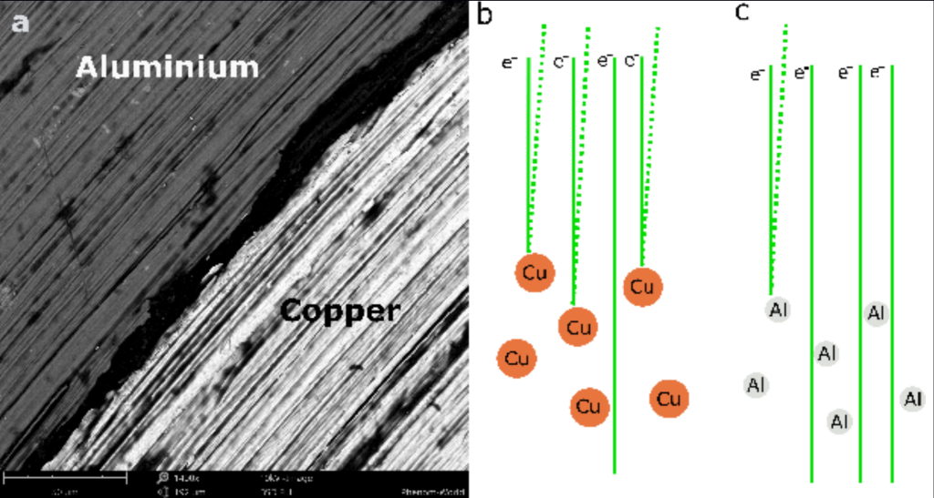
Larger atoms scatter electrons much more strongly than lighter atoms and therefore produce higher signals (Figure 2). The number of backscattered electrons reaching a detector is proportional to its Z number.
This dependence of BSE amount on atomic number helps to distinguish different phases, providing imaging that conveys information about the sample composition.
In addition, BSE images can provide useful information about the sample’s morphology, crystallography, and magnetic field.
Solid state detectors are the most common BSE detectors and usually contain a pn junction. Its working principle is based on the creation of electron-hole pairs from backscattered electrons that escape the sample and are captured by the detector. The number of these pairs depends on the energy of the backscattered electrons.
The pn junction is connected to two electrodes, one of which attracts electrons and the other attracts holes, thus generating an electric current, which also depends on the number of backscattered electrons absorbed.
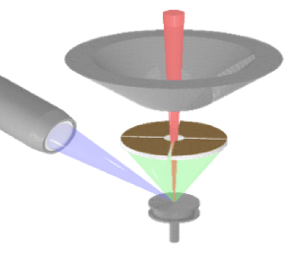
The BSE detector is located above the sample, concentric with the electron beam, in a “doughnut” arrangement to maximize the collection of backscattered electrons, and they consist of symmetrically separated sections.
When all sections are enabled, the contrast of the image shows the atomic number Z of the number. Alternatively, topographic information can be recovered from an image by enabling only specific quadrants of the detector.
Secondary electronics
Secondary electron imaging is to use the electron imaging of the outer layer of the sample bombarded by the incident electrons. The energy is low, and it can only characterize the surface of the sample, and the resolution is relatively high.
Backscattered electrons are incident electrons scattered by the sample and then imaged, with high energy close to the incident electrons. It can reflect the deep information inside the sample, and the resolution is relatively low.
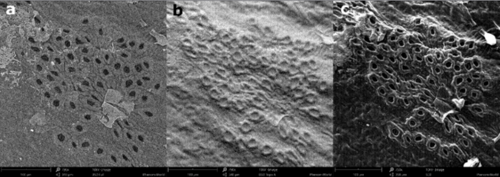
Secondary electrons come from the surface 5-10nm region with energies of 0-50eV. It is very sensitive to the surface state of the sample and can effectively display the microscopic topography of the sample surface.
Since it is emitted from the surface of the sample, the incident electrons have not been reflected many times, so the area where the secondary electrons are generated is not much different from the area irradiated by the incident electrons, so the resolution of the secondary electrons is relatively high, generally reaching 5-10nm.
The resolution of the scanning electron microscope is generally the secondary electron resolution. The secondary electron yield does not change much with the atomic number, it mainly depends on the surface topography.
The incident electrons collide with the extranuclear electrons of the sample, and the extranuclear electrons on the sample surface are excited. The electrons are used as the imaging signal of the SEM and represent the structural characteristics of the sample surface.
The secondary electrons originate from the surface or near-surface regions of the sample. They arise due to the inelastic interaction between the primary electron beam and the sample and contain lower energy than backscattered electrons. As shown in Figure 4, secondary electrons are very beneficial for the inspection of the sample surface topography.
The Everhart-Thornley detector is the most commonly used device for detecting SE. It consists of a scintillator inside a Faraday cage, which is positively charged and attracts SE. A scintillator is then used to accelerate the electrons and turn them into light, which then reaches a photomultiplier tube for amplification. The SE detector is positioned on one side of the electron chamber and is angled to improve the efficiency of detecting secondary electrons.
These two types of electrons are common signals used by SEM users for imaging. Not all SEM users need the same type of information, so the ability to have multiple detectors makes SEM a highly versatile tool that can provide beneficial solutions for many different applications.