Transmission Electron Microscope (TEM) generally uses the interaction between the light mode of the electron light source and the sample to be measured, which is parallel to the optical axis or converged at a certain point on the optical axis, to the image. The parallel light is regarded as the light source of the flashlight, and the converging light is regarded as the light source of the laser.
Lighting system
The illumination system receives the beam from the electron gun and directs it to the sample, either in the form of a wide “parallel” beam for TEM, or a small focused probe for STEM. For this, the combination of two condenser lenses and at least one aperture at the exit plane of the second condenser lens (combined with tilt and deflection coils) is required.
In TEM mode, adjust the condenser lens to form a wide beam of several micrometers in diameter on the sample [3]. The upper pole piece of the objective can act as a third condenser to produce a more parallel beam. This is ideal for producing sharp diffraction patterns and greater image contrast.
Comparison of TEM and STEM illumination for forming parallel beams or converging probes, respectively, at the sample inlet surface.
For STEM patterns, the opposite is required. Instead, the illumination system acts to create a converging light beam (probe) at the sample inlet surface. An image is formed by scanning a focused probe across the field of view. Insert the condenser aperture to define the convergence angle α of the probe.
Parallel light irradiation mode (TEM)
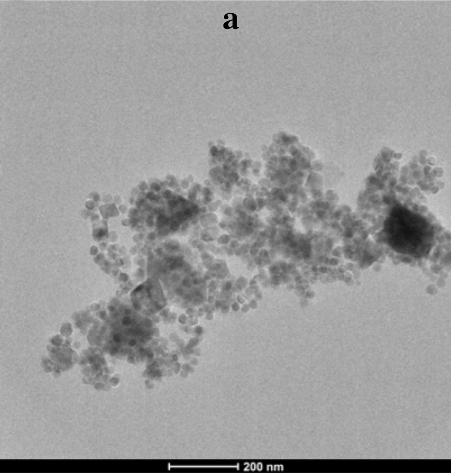
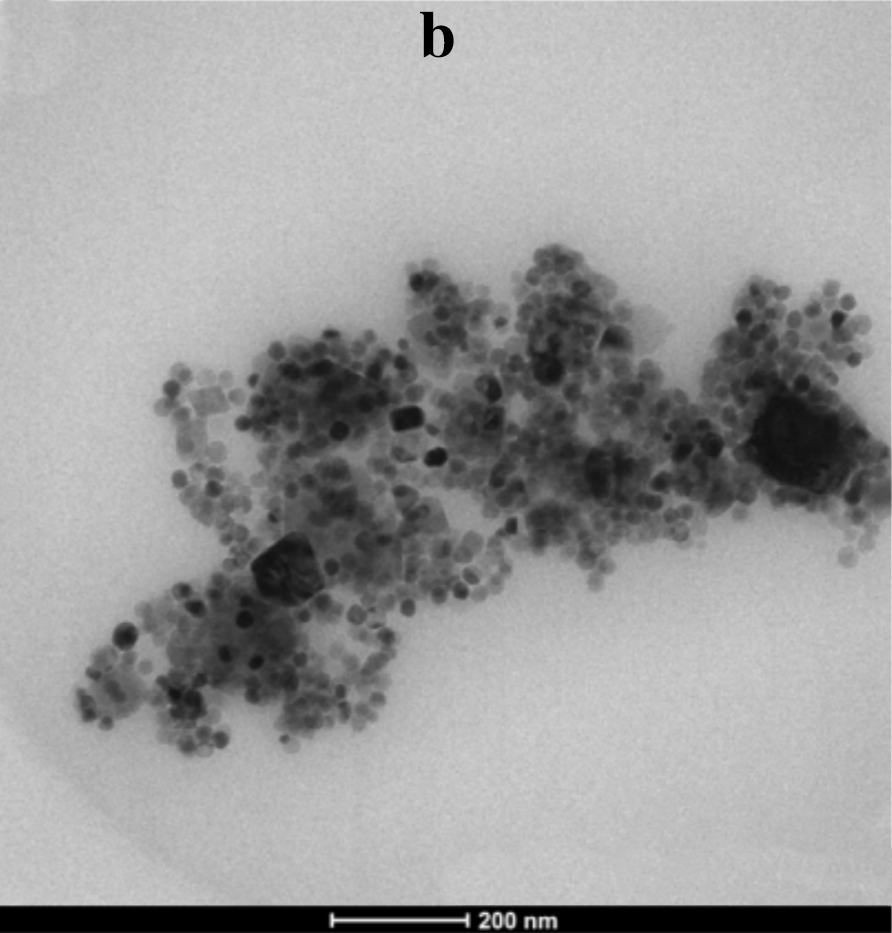
Parallel light mode (TEM) light is planar and has a large range. In daily testing, it is mainly used to observe the microscopic morphology and structure of the sample, such as the profile of the catalyst powder, the size of the nanoparticles, the distance between the crystal planes, and the arrangement of atoms.
1. TEM bright and dark field contrast image
Bright-field imaging: On the back focal plane of the objective lens, the transmitted beam passes through the aperture of the objective lens to block the diffracted beam to obtain an image.
Darkfield imaging: the direction of the incident beam is tilted at an angle of 2θ, and the transmitted beam is blocked by the diffracted beam through the objective lens diaphragm to obtain an image.
2. High-resolution TEM (HRTEM) images
HRTEM is a phase contrast image, which is the interference image produced by all the diffracted beams and transmitted beams participating in the imaging due to the phase difference. It is used to observe the internal structure of the crystal, atomic arrangement, and many fine structures (such as dislocations, twins, etc.) Higher resolution images information such as lattice fringe image, structure image, and single atom image can be obtained.
The shooting of high-quality HRTEM images requires high-demand samples to be tested:
1) The sample is thin enough (weak phase approximation) with a thickness of less than 10 nm;
2) The sample must be stable and firm on the copper grid so that it can withstand the bombardment of the electron beam and prevent damage due to mechanical vibration during loading and unloading.
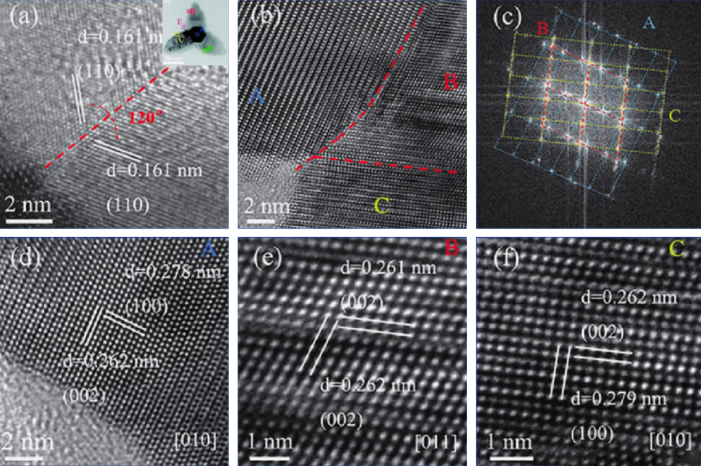
(a) HRTEM image of the interface between two feet when the electron beam is incident along the long axis of a foot
(b) HRTEM image of the interface between each foot after (a) was tilted 30°
(c) The FFT diagram corresponding to Figure (b)
(d)-(f) are the HRTEM images of marks A, B, and C in (b) respectively
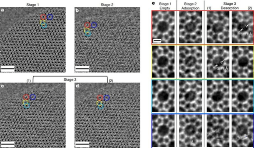
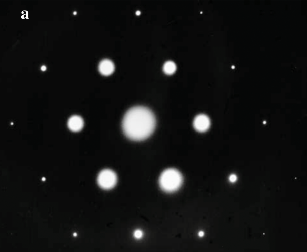
3. Selected area electron diffraction image
Selected area electron diffraction (SAED) imaging refers to the method of using the TEM imaging optical path to carry out diffraction operation to project the shooting pattern from the diffraction pattern on the back focal plane of the objective lens to the fluorescent screen. Photographing SAED can obtain structural features in the micron range to characterize the material structure. The image acquisition area is determined by the magnification of the objective lens and the size of the selected aperture, the polycrystal is the diffraction ring, and the single crystal is the diffraction point.
4. Spectral image
Energy-dispersive X-ray spectroscopy (EDS) is the most commonly used method for micro-area composition analysis. Based on the characteristic X-rays of the sample to be tested, information of the elements existing in the analyzed area and the relative composition of each element can be obtained. content. In the TEM parallel light mode, the collected X-rays characteristic of elements are expanded into a spectrum according to the energy, and the energy corresponds to the peak of the element, and the peak area ratio is the element content ratio.
Concentrated light irradiation mode (STEM)
Converged light (STEM) imaging is different from parallel photoelectron beams. It is realized by scanning the sample point by point with the concentrated electron beam. If it is necessary to directly reflect the atomic information of the sample or EDS-Line Scan, EDS-Mapping, and STEM- When analyzing components with low EELS concentrations, STEM imaging can be selected.
The HAADF-STEM image is most commonly used in the STEM mode. The intensity of the image is proportional to the square of the atomic number Z, and the larger the Z, the brighter the image. During the test, the HAADF probe is used to collect sample information, and the atomic and composition information of the sample can be collected.
The STEM mode can also be used for imaging such as Convergent beam electron diffraction (CBED), BF-STEM (Bright field image), and ADF-STEM (Annular dark field image).
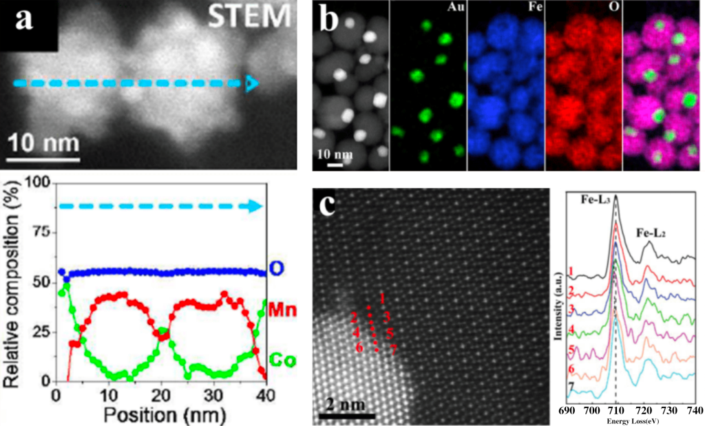
(b) High-angle annular dark field image (HAADF) of Au/Fe3O4 heterostructure nanoparticles and EDS-Mapping of the corresponding particles
(c) EELS spectra of atomic pillar iron ions at the Au/Fe3O4 heterostructure interface
Frontline application of TEM
In addition to the above-mentioned common functions, along with the advancement of technology, different research, and transformations have been carried out on the basis of the basic functions and structures of TEM, so that the front-line application of TEM has been explored and developed. For example, 3D-tomography technology in situ explores the changes of matter in physical fields such as optics, electricity, magnetism, mechanics and temperature, and gas/liquid state, and observes soft matter materials, which are not resistant to electron beam irradiation to destroy more atomic information of materials. Such as iDPC-STEM technology.