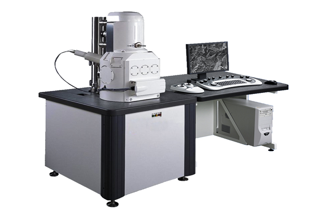
The theory of image formation in electron microscopy is very similar to that in optical microscopy. However, practice and design are completely different: the most crucial difference is that lighting is a beam of electrons rather than light.
Due to the mass of electrons being greater than light, their energy is higher and their wavelength is shorter, thus achieving higher resolution (as low as 1 nm).
Unlike light, electrons only travel directionally when accelerated through voltage gradients in a high vacuum.
Electric and magnetic fields must be used instead of refractive and reflective materials such as glass to focus electrons. Electrons also only interact with heavy atomic nuclei (>20 amu) (scattering).
The main focus of traditional electron microscopes is on preparing samples, which allows them to be imaged in an electron beam.
Biologists rarely break through the resolution limits that electron microscopes can achieve.
Transmission electron microscopy (TEM)
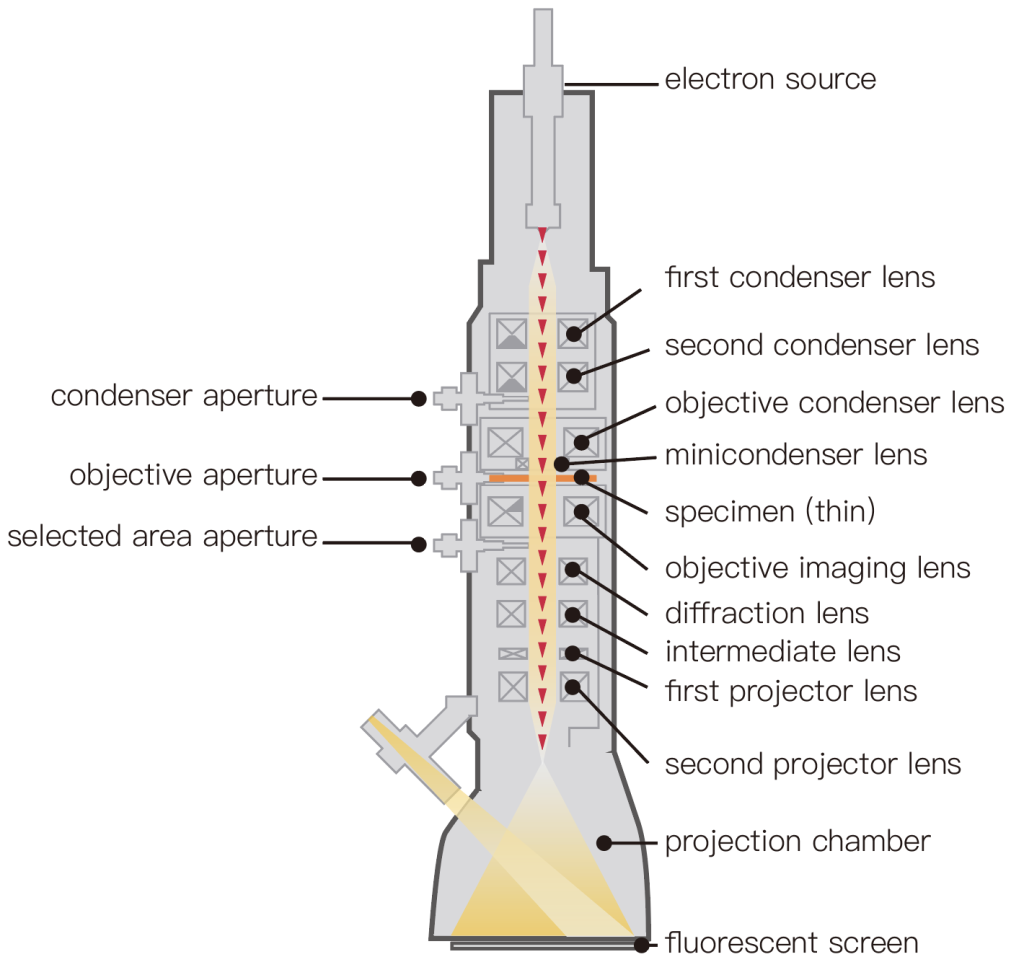
Transmission electron microscopy (TEM) is a wide-area imaging technique that is conceptually similar to the bright field in optical microscopy.
The filament generates free electrons and focuses on the sample using an electromagnetic focusing lens system. Then, electrons passing through the sample are used to form the image.
Some transmitted electrons are scattered by metal atomic spots in the sample. The more scattering occurs the darker the area in the final image.
Phase imaging based on electrons interacting with the sample is also possible, but it is not common in biological applications.
After passing through the sample, the electromagnetic objective system refocuses the electrons, usually onto a fluorescent screen, which converts the electron image into the light.
Finally, optical devices are used to focus phosphorescent photons onto standard CCD or CMOS cameras.
Advantages:
Very high (<1 nm) resolution
Disadvantages:
Sample preparation requires a long and complex process, including fixation, dehydration, and heavy metal staining, as well as ultra-thin sections before imaging. The cross-section is very two-dimensional (50-100 nanometers thick), making it difficult to appreciate complex 3D objects.
Common applications:
The accelerated voltage of 60-80 keV: High magnification imaging of ultra-thin sections of single-layer cell or tissue specimens. 100 keV accelerating voltage: high magnification imaging of proteins, nanoparticles, microorganisms, and organelle.
The acceleration voltage of 200 or 300 keV: Used for high magnification imaging of TEM array tomography and thin slice high angle tilt tomography.
TEM tomography scans perform a series of TEM images on the sample at many different tilt angles.
Using tomographic reconstruction methods, 3D images can then be reconstructed from oblique sequences. The larger the range of tilt angle, the higher the resolution that can be achieved.
A larger angle also means that the electron beam must pass through the sample at a highly inclined angle, thus traversing a longer distance within the sample. A higher acceleration voltage is required to penetrate more samples (such as 300 keV).
Scanning electron microscopy
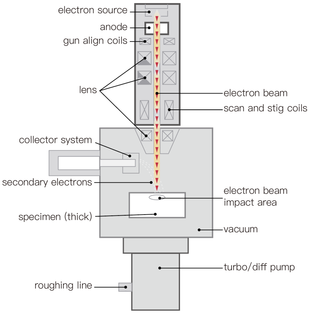
Scanning electron microscopy provides information about surface morphology and, in some cases, surface composition. Unlike a transmission electron microscope that illuminates the entire sample at once (with a wide field of view), a scanning electron microscope is a point scanning technique that quickly scans a single electron focal point on the sample in a grating mode to collect images in chronological order.
The scanned electrons then interact with the sample and generate various signals, which can be detected to create an image. Three types of signals are commonly used in biological SEM imaging applications:
Secondary electron (SE) imaging is based on the electrons emitted from the sample after being impacted by an electron beam. The SE signal originates from the surface of the sample and mainly provides information about surface morphology.
Backscattered electron (BSE) imaging is based on electrons penetrating the sample and colliding with atomic nuclei. Therefore, BSE images mainly provide information about the atomic number and density difference: the higher the atomic number, the brighter the material appears in the image because more beam electrons are backscattered.
Energy dispersive X-ray spectroscopy (EDS, EDX, or XEDS) imaging is based on the detection of X-rays (high-energy light) generated when electrons are emitted from the sample by an electron beam. When sample electrons from other energy levels fill these “holes”, characteristic X-ray energy is generated, similar to fluorescence in an optical microscope. Then, the measured X-ray energy provides information about the local atomic energy levels, which can be used for elemental analysis or chemical characterization of the sample.
Advantages:
High-resolution (2-10 nm) information about the surface of the sample.
Disadvantages:
There is no information about the interior of the sample (>10 nm deep).
Common applications:
Surface information is required at any time.
Focused ion beam scanning electron microscopy (FIB-SEM) is a continuous block imaging technique used to create 3D SEM images. Ion beams (Ga or Xe) are used to finely grind the surface of the sample (5 to 10 nm per cut). After each milling, the newly exposed block surface is imaged in SEM mode. Repeat this process over and over again to slowly create a 3D image of the sample. Please note that this method is destructive as the sample is ground off at each step.
Advantages:
High (2-10 nm) resolution in the xy and z directions.
Disadvantages:
A very expensive instrument, milling means that the sample is destroyed during the imaging process. Due to slow collection, it is actually limited to small areas (4 x 4 x 2 um).
Common applications:
When high-resolution 3D images are required. To achieve higher resolution but a smaller depth, consider TEM tomography imaging. For lower resolutions, please consider array tomography or knife-based serial block facial imaging.
Array tomography is actually a sample serial slicing technique, but it can achieve 3D EM imaging at low (500-100 nm) z resolution. Use a special ultra-thin slicer to continuously slice up to 100 resin-embedded samples. Then place the slices on silicon wafers for SEM imaging or slotted grids for TEM imaging. After obtaining the 2D image of the slice, the software is used to fully align the image into the 3D image.
Advantages:
Large field of view in xy at lower resolutions (100s um). The serial port will not be damaged during the imaging process.
Disadvantages:
Reliable cutting of many continuous ultra-thin slices is very difficult and labor-intensive. Due to geometric distortion, image processing may also be difficult.
Common applications:
Low-resolution 3D image reconstruction.