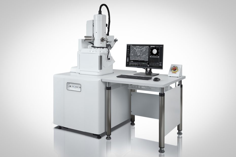
Before we dive into the topic of SEM microscope resolution, let’s take a step back and explain how an SEM works.
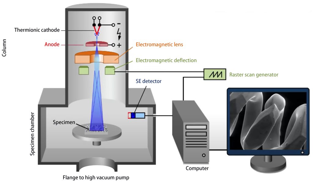
A scanning electron microscope scans a focused beam of electrons over the surface of a sample to create a magnified image. Electrons in the beam interact with the sample, generating multiple signals. These signals allow materials science researchers to obtain information about material composition and surface topography.
SEM is widely used in various fields such as scientific research and industry because of its simple sample preparation, large image field of view, long depth of field, strong three-dimensional image, and the ability to receive and analyze most of the information generated by the interaction between electrons and samples.
However, the scanning electron microscope is a very precise instrument with a complex structure. It is still very difficult to obtain high-quality images that can fully reflect the material morphology, clear layers, strong three-dimensional effect, and high resolution.
Resolution is the basic performance judgment index of a scanning electron microscope (SEM). For imaging, it refers to the minimum distance between two points that can be resolved; for micro-area component analysis, it refers to the smallest area that can be resolved. The smaller the resolution distance or area, the better the performance and the higher the resolution.
Because the wavelength affects the limited theoretical resolution of the electron microscope, but in actual use, other factors often have a greater impact.
The maximum SEM resolution depends on several factors, including the size of the incident electron beam and the interaction volume of the electron beam with the sample.
In general, the resolution of a scanning electron microscope can be affected by the following factors:
A. Incident electron beam spot diameter
is the limit of the resolving power of the scanning electron microscope. Generally, the minimum beam spot diameter of the hot cathode electron gun can be reduced to 6nm, and the field emission electron gun can make the beam spot diameter smaller than 3nm.
B. Spreading effect of the incident electron beam in the sample
The degree of diffusion depends on the energy of the incident beam electrons and the atomic number of the sample. The higher the energy of the incident beam, the smaller the atomic number of the sample, the larger the volume of the electron beam, and the area where the signal is generated increases with the diffusion of the electron beam, thereby reducing the resolution.
C. Imaging methods and modulation signals used
When the secondary electron is used as the modulation signal, due to its low energy (less than 50eV) and short mean free path (about 10-100nm), only the secondary electrons within the depth range of 50-100 nm in the surface layer can escape the sample surface, the number of scattering occurrences is very limited and basically does not expand laterally.
Therefore, the secondary electron image resolution is approximately equal to the beam spot diameter. When the backscattered electrons are used as the modulation signal, the energy of the backscattered electrons is relatively high and the penetrating ability is strong, so they can escape from a deeper area in the sample (about 30% of the effective depth).
In this depth range, the incident electrons have a fairly wide lateral expansion, so the resolution of the backscattered electron image is lower than that of the secondary electron image, generally around 500-2000nm.
If other operation modes such as absorbing electrons, X-rays, cathode fluorescence, beam-induced conductance or potential are used as modulation signals, since the signals come from the entire electron beam scattering area, the resolution of the obtained scanning images is relatively low, generally at 1000 nm or Above 10000nm.
Summarize
Thanks to the nanoscale resolution of scanning electron microscopy, SEM opens up a whole new world for researchers. For example, viruses range in size from 60 to 140 nanometers. A DNA strand has a radius of one nanometer. Glucose molecules are about 0.9 nanometers in size. You can solve all these problems with SEM.
In materials science research, you can easily examine metals, alloys, polymers, ceramics, electronics, particles, and organic materials, and nanometer feature sizes can be examined due to the high resolution of the SEM.