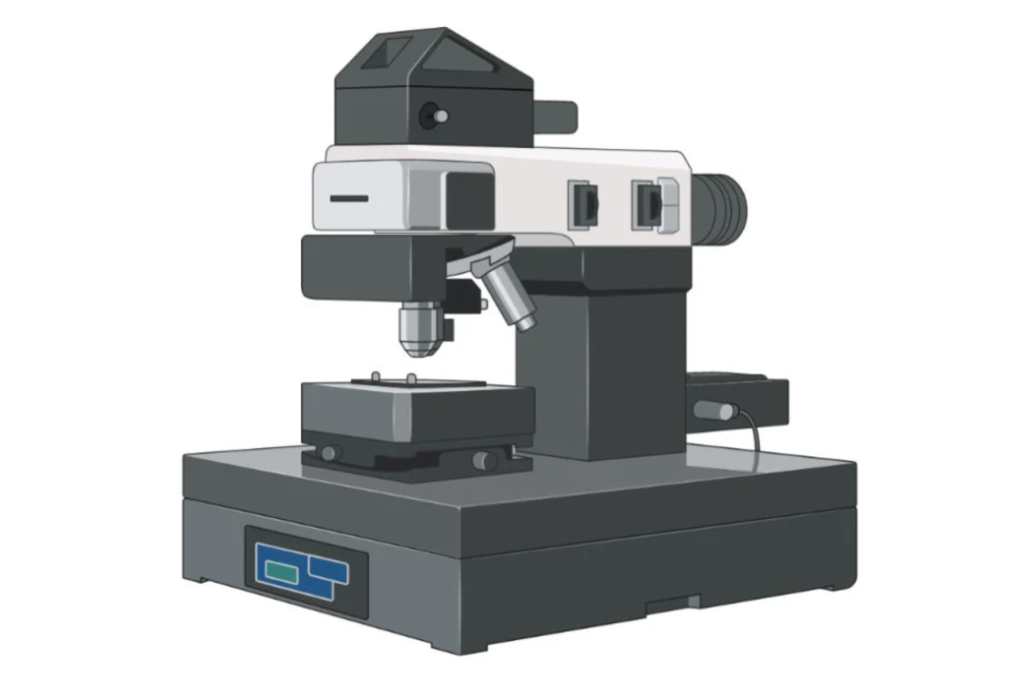
Atomic Force Microscope (AFM) is a new type of high-resolution microscopy instrument invented after the scanning tunneling microscope. It has atomic-level recognition capabilities and can be used in a variety of environments (air or solution environments). ) Observe and detect various materials and samples at the nanometer level, including detecting surface morphology and measuring surface roughness at the nanometer level.
At present, AFM (atomic force microscope) has been widely used in various fields, including semiconductors, nanofunctional materials, biology, chemical industry, medicine, and other research fields, and has become one of the indispensable tools in scientific research.
Basic principles of atomic force microscopy
One end of a tiny cantilever that is extremely sensitive to weak force is fixed, and the other end contains a tiny tip. During the test, the tip gently touches the surface of the sample to be tested. Since the atoms at the tip of the tip are in contact with the sample to be tested, There is an extremely weak interaction force between atoms on the surface of the sample to be measured. By maintaining this interaction force constant during scanning, the micro-cantilever with the tip and the surface of the sample to be measured performs an undulating motion in the direction perpendicular to the surface of the sample.
Finally, through the method of optical detection or tunnel current detection, the changes in the position of each scanning point can be observed, so that information such as the surface morphology of the sample can be accurately obtained.
Application scenarios of atomic force microscope
Surface topography and surface roughness
By detecting the force between the probe and the sample, the three-dimensional topography of the sample surface can be characterized, which is the basic function of AFM (atomic force microscope). The morphology of the sample can also be displayed in rich three-dimensional simulations, making the image more suitable for human intuitive vision. The figure below represents the two-dimensional geometric topography and three-dimensional height topography of the sample. The height image of AFM (atomic force microscope) can be used for high-resolution roughness measurement of micro-regions on the sample surface. Using appropriate data analysis software, the statistical results of each characteristic parameter of roughness in the measured area can be obtained.
Surface average roughness Ra and root mean square roughness Rq are commonly used parameters to characterize roughness. Their meanings are: Ra refers to the arithmetic mean of the absolute value of the height deviation measured relative to the central plane in the area under investigation, and Rq is It refers to the root mean square value of the contour deviation from the average line within the sampling length, which is the root mean square parameter corresponding to Ra. The computer can automatically calculate the arithmetic mean deviation Ra and root mean square roughness Rq of the contour based on the height data.
The 2D main topography and 3D main topography of the sample and the roughness values Ra and Rq of the sample
Measurement of step height and nanosheet thickness
During semiconductor processing, it is often necessary to measure high aspect ratio structures like trenches and steps to determine the depth and width of etches. These can only be measured under SEM by cutting the sample along the cross-section. AFM (atomic force microscope) can measure it non-destructively. At the same time, the resolution of AFM (atomic force microscope) in the vertical direction is about 0.01nm, so it can be very good. Used to characterize nanosheet thickness.
Step height (left) and nanosheet thickness (right) measurements
Phase Diagrams
The phase diagram is a comprehensive reflection of surface mechanical information. Various properties such as surface elasticity, viscosity, electromagnetic properties, friction, etc. will cause changes in the phase diagram. It is meaningless to analyze the image obtained by the phase mode alone. It must be combined with the topography map and the two images can be compared and analyzed to obtain the required information.
To put it simply, if the contrast between two materials is relatively small in terms of AFM (Atomic Force Microscopy) morphology, but you really want to explain what kind of film it is grown on, you can use the two-dimensional morphology diagram + Phase diagram is used to illustrate (the premise is that the physical properties of the two materials are relatively different, and the phase diagram has obvious contrasting signals).
Main morphology and phase diagram of the sample
Force curve
On the base slope (Ramp), set the parameters to get the force curve. The abscissa of the curve is the relative distance change between the probe and the sample. The ordinate is the force between the probe and the sample. The blue line is the probe pressing into the sample. Curve, the red line is the curve leaving the sample. The ordinate line shows how the force between two atoms (between the probe and the sample) changes with distance. It has two components, one is a positive component and the other is a negative component. Positive values represent repulsion and negative values represent attraction.
Through force curve analysis, it can be obtained:
- 1 Peak force (maximum force of probe sample)
- 2 Adsorption force (minimum force of probe sample)
- 3 Young’s modulus
- 4 Deformation amount of probe sample
- 5 Energy dissipation
- 6 Elastic modulus: generated when the probe contacts the sample on the curve During repulsion, the relationship between the distance the probe descends and the force is linear. This rule can be used to simulate and calculate the elastic modulus of the sample surface;
- 7 Adhesion force: During the process of the probe leaving the sample, the adhesion force is involved, and the curve is the lowest Point that can be used to obtain the size of the adhesion force on the sample surface;
- 8 Work of adhesion: The integral of the overlapping area of the curves is the work done by the adhesion force.
Force curve analysis
QNM Young’s modulus test
Atomic force microscopy testing and quantitative characterization of microscale mechanical properties.
QNM Young’s modulus test
EFM electrostatic force test – relative electrostatic force strength distribution
Characterize the electrostatic potential energy, charge distribution and charge transport on the sample surface.
EFM electrostatic testing
KPFM surface potential test – measuring the potential difference between two phases
On the basis of obtaining the surface morphology of the sample, the surface work function or surface potential can be obtained at the same time.
KPFM surface potential test
PFM Piezoelectric Characteristics Test-Write Domain/Return Word (Piezoelectric Material)
It is used to study the surface potential and piezoelectric response measurement of piezoelectric materials, ferroelectric materials, and multiferroic materials at the nanoscale. It mainly detects the electrical deformation of the sample under external excitation voltage.
PFM Piezoelectric Characteristics Test