Nanotechnology is the foundation of future high-tech development. The chemical composition, structure and microstructure relationship of nanomaterials are the key factors that determine their performance and application. Instrumental analysis methods that can be used for nanomaterial characterization have become indispensable in nanotechnology. experimental means. Many researchers and related personnel are not very familiar with nanomaterials, especially how to analyze and characterize nanomaterials and obtain some characteristic information of nanomaterials.
Visualization and imaging of nanomaterials is critical to characterize and obtain critical information about nanostructures. Optical microscopy offers the opportunity to observe, visualize and capture images of nanoparticles, which helps advance nanotechnology.
This article discusses the applications of light microscopy for analysis, visualization, and imaging of nanomaterials, as well as its limitations.
What is an Optical Microscope?
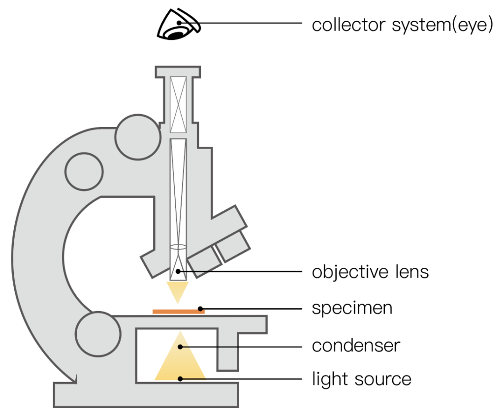
A light microscope is a microscope that uses different lenses and visible light to magnify small samples. Optical microscopes are the oldest microscopes.
The most basic light microscope can be very simple. However, many complex designs are aimed at improving resolution and sample contrast. Historically, these microscopes were easy to manufacture. They are still popular today because they utilize visible light and allow the naked eye to view materials.
How is light microscopy used for visualization and imaging?
Optical visualization is a very effective method to obtain information about the morphology of materials. With the help of optical visualization technology, real-time color real-time images can be collected, which is conducive to observing dynamic processes. Compared with scanning probe microscopes and electron microscopes, optical microscopes are gentle, simple, and low-cost for visualization.
To make photomicrographs, the images seen through an optical microscope can be captured by a conventional light-sensitive camera. In light microscopy, conventional photographic film is used for imaging. However, technological developments in complementary metal-oxide-semiconductor and charge-coupled device (CCD) cameras have made digital imaging possible.
Fully digital optical microscopes and CCD cameras are now available. These digital light microscopes bypass traditional eyepieces, and images can now be seen directly on a computer screen.
How is Optical Microscopy Used for Nanomaterials Analysis?
For the characterization of nanomaterials, the ability to directly observe nanoparticles under ambient conditions is very important. Typically, to observe individual nanoparticles, high-resolution electron microscopy under high vacuum is required.
Optical microscopes are used for the characterization and analysis of nanomaterials due to their open spaces and easy handling. However, there is a significant difference in resolution between light and electron microscopes. Therefore, efficient imaging and visualization are required for controlled manipulation, precise localization, and direct observation of nanoparticles.
Examples of Optical Microscopy for Analyzing Nanomaterials
Over the past few years, various different methods for analyzing nanomaterials by optical microscopy have been proposed. For example, researchers have made significant progress in optically visualizing various nanomaterials, such as nanofibers, graphene, and carbon nanotubes, by depositing visible “tags” or exploiting certain optical phenomena.
These efforts paved the way for further research on the properties and applications of these nanomaterials. In addition, optical microscopy enables scientists to directly manipulate nanomaterials by designing and modifying the setup. This not only expands the range of applications, but also leads to a better understanding of nanoscale dynamic processes.
Different types of optical microscopes are used to characterize and analyze nanomaterials. For example, photothermal optical microscopy, Raman microscopy, surface plasmon resonance microscopy, dark-field microscopy, and fluorescence microscopy are used in nanocatalysis, nanoelectrochemistry, and nanosensing to obtain key information about different nanostructures.
Limitations of Optical Microscopy
One of the limitations of optical microscopy is the low resolution, as well as the enormous beam size of the optical microscope. This limitation is disadvantageous, especially for imaging nanomaterials, since the size of many nanoparticles, nanotubes, or nanostructures is much smaller than the optical resolution limit of 200 nm.
For example, the visualization of carbon nanotubes (CNTs) is impossible with ordinary light microscopy because the diameter of CNTs is usually much smaller than the size of the illuminating beam. Therefore, effective imaging and visualization strategies need to be carefully designed to enable their direct observation, subsequent utilization, performance characterization, controllable manipulation, and precise localization.