Photovoltaic systems, also known as photovoltaics, referred to as photovoltaics, refer to facilities that convert solar energy into DC power by using the photovoltaic effect of photovoltaic semiconductor materials.

At the heart of a photovoltaic installation are the solar panels. At present, the semiconductor materials used for power generation mainly include: single-crystal silicon, polycrystalline silicon, amorphous silicon and cadmium telluride. As countries in recent years are actively promoting the application of renewable energy, the development of the photovoltaic industry is very rapid.
As the core component of photovoltaic power generation, solar photovoltaic cells have attracted much attention for their development prospects and market value. Photovoltaic cells account for about 27% of the global sales revenue of various battery products. Scanning electron microscopy plays a huge role in improving the production process of photovoltaic cells and related research.
Photovoltaic cells are thin sheets of optoelectronic semiconductors that convert sunlight directly into electricity. At present, the commercialized large-scale production of photovoltaic cells is mainly based on silicon cells, which are divided into monocrystalline silicon cells, polycrystalline silicon cells and amorphous silicon cells.
Texturing to improve the absorption efficiency of solar cells
In the actual preparation process of photovoltaic cells, in order to further improve the energy conversion efficiency of the battery, a special layer of suede structure is usually made on the surface of the battery. The battery made of suede is called a “texture battery” or “non-reflective”. Battery.
Specifically, the textured structure on the surface of these solar cells can not only reduce the reflectivity of the surface but also form light traps inside the cell by increasing the number of reflections of the irradiated light on the surface of the silicon wafer and improving the light absorption rate, thereby significantly It is of great significance to improve the efficiency and reduce the cost of existing silicon photovoltaic cells.
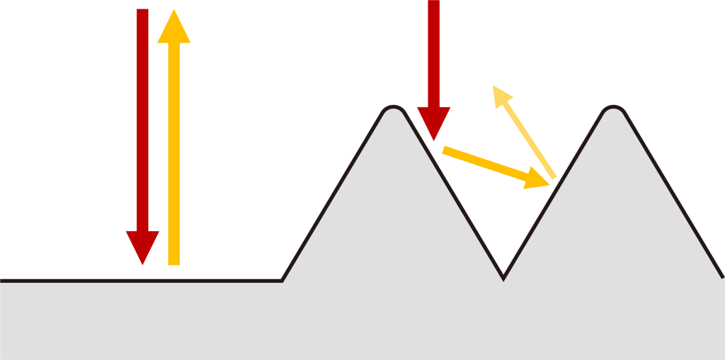
Compared with a flat surface, a silicon wafer with a pyramid structure texture has a greater probability that the reflected light generated by the incident light will act on the surface of the silicon wafer again instead of directly reflecting back into the air, thereby increasing the scattering of light on the surface of the structure And the number of reflections, so that more photons are absorbed and more electron-hole pairs are provided.
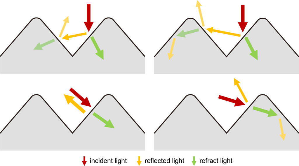
At present, the existing surface texturing methods include: the chemical etching method, reactive ion etching method, a photolithography method, mechanical groove method, etc. Among them, the chemical etching method has been widely used in the industry because of its low cost, high productivity and simple method. For monocrystalline silicon photovoltaic cells, the anisotropic etching produced by alkaline solution in different crystal orientations of crystalline silicon is usually used to form a textured surface similar to a “pyramid” structure on the surface of the silicon wafer. The formation of the pyramid structure is due to the anisotropic reaction of alkali with silicon. In a certain concentration of alkaline solution, the reaction speed between OH- and Si(100) surface is several times or even ten times faster than that of Si(111) surface. It is precisely because of this reaction speed difference that the pyramid structure is formed.
Scanning Electron Microscope Helps Improve Quality of Solar Cells
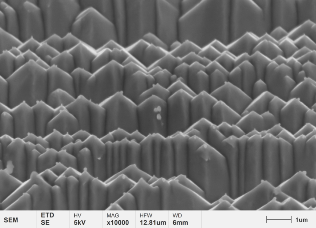
In the process of chemical etching, factors such as the concentration of the etching solution, temperature, and reaction time will affect the preparation of the surface of the silicon crystal cell wool, resulting in a difference in reflectivity. Using a tungsten filament scanning electron microscope can analyze the corrosion area in the production process. Effective observation of size, surface pyramid structure, etc.
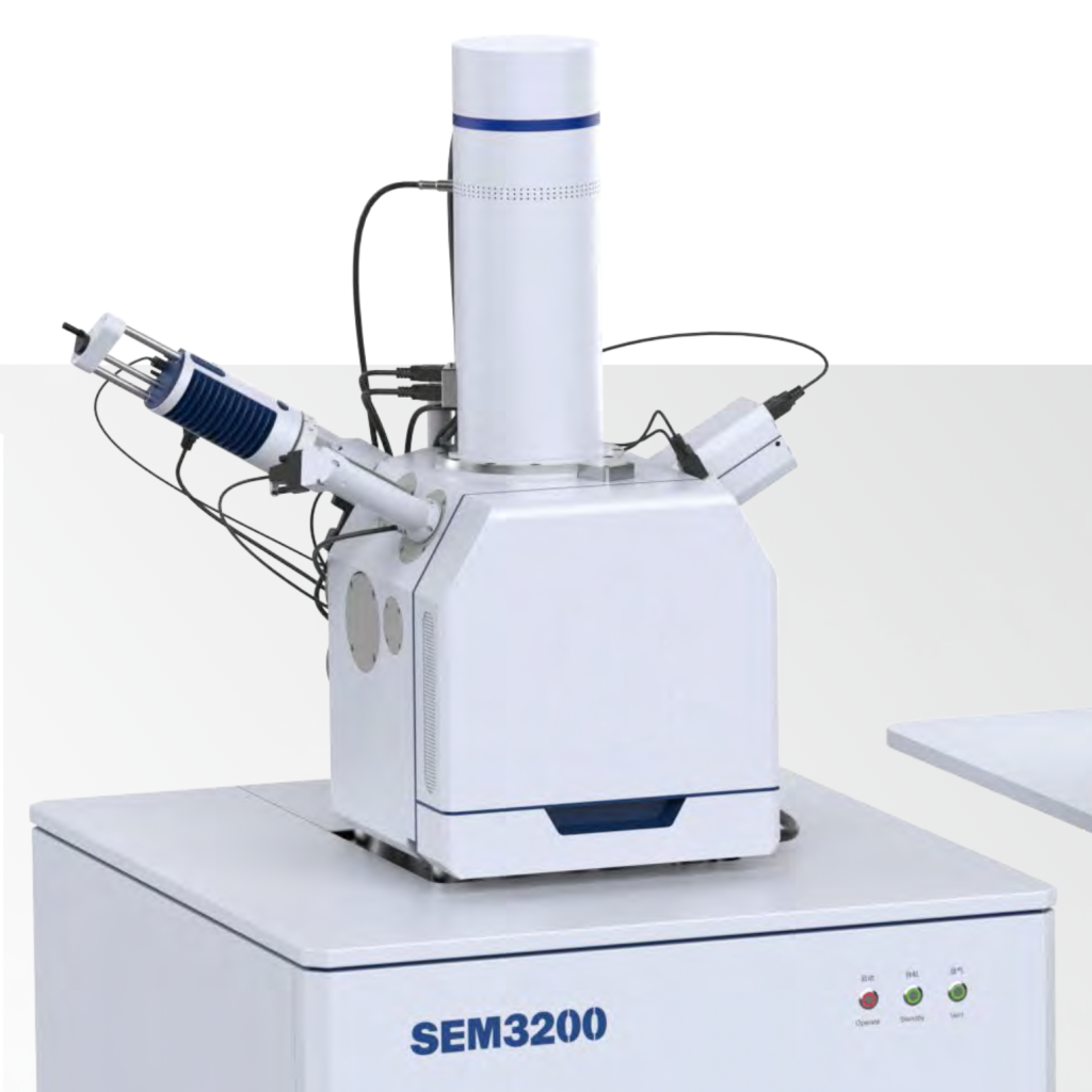
Thanks to the advantages of the large-capacity sample chamber of the SEM3200 electron microscope, users can put photovoltaic cell samples with a maximum diameter of 370mm without cutting during use, and the five-axis fully automatic sample stage on the electron microscope can achieve -10°~75° ° tilt, can realize multi-angle observation of different positions of the sample.
The appearance of suede after the sample stage is tilted 45°
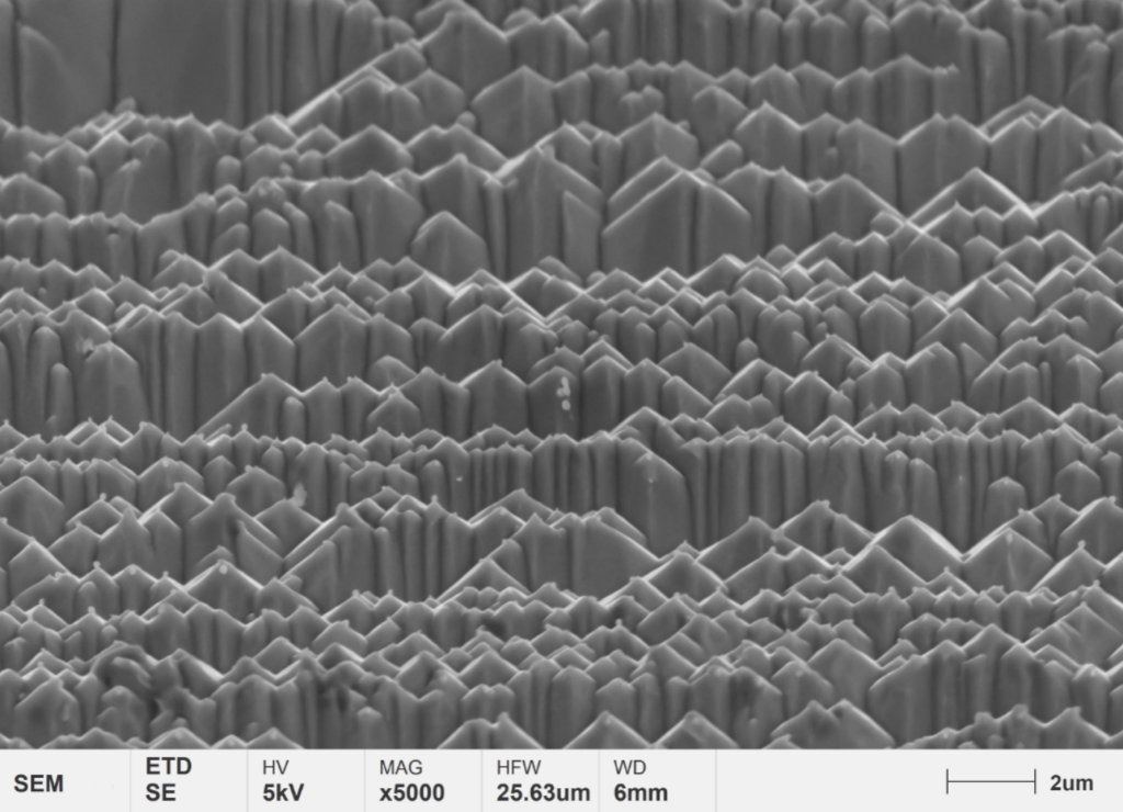
The appearance of suede after the sample stage is tilted by 30°

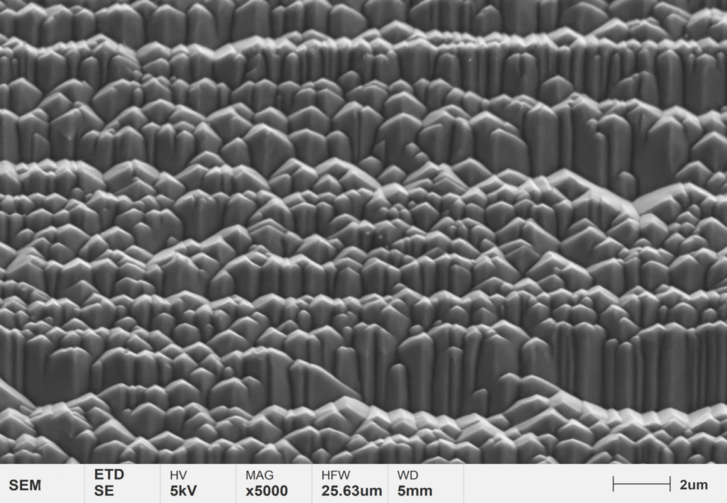
Observation of samples placed horizontally
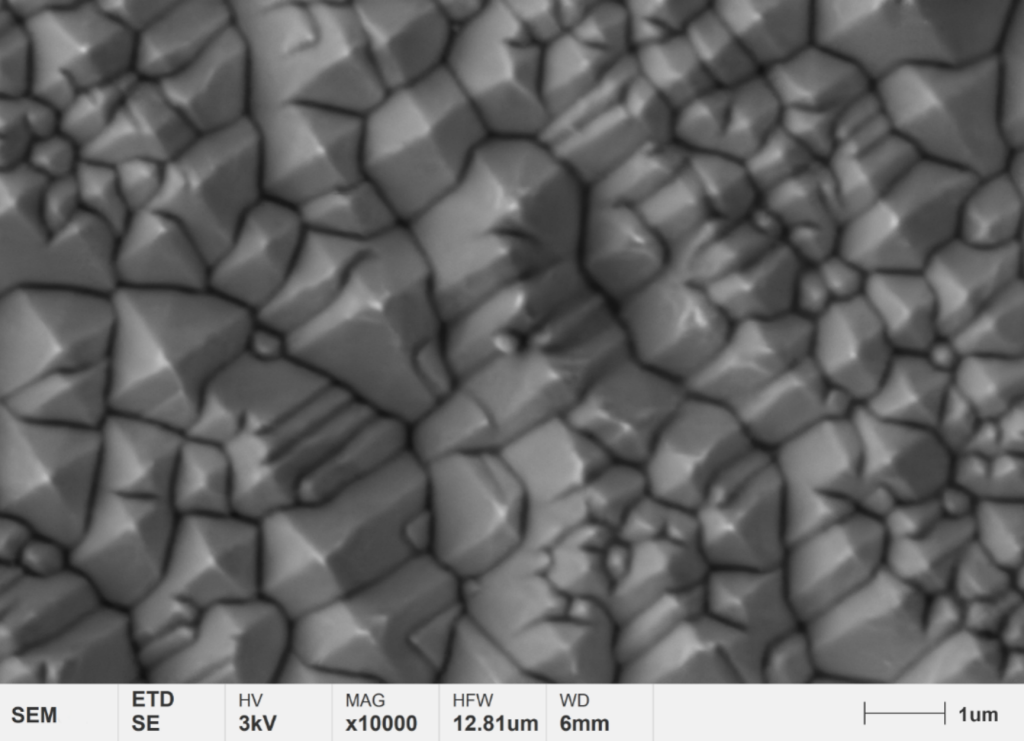
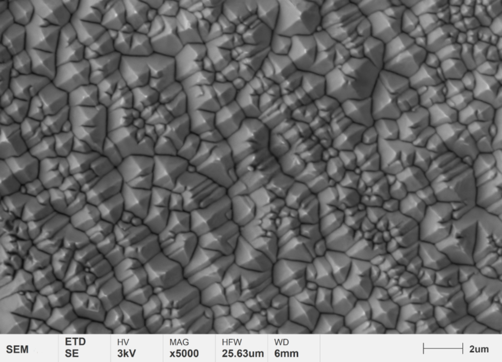
Using the SEM3200 electron microscope to observe the pyramid structure on the surface of photovoltaic cells with a lower accelerating voltage of 3~5kV can reduce the penetration depth of the electron beam on the surface of the sample, making the observed surface details more abundant, and better understanding surface defects and structures. Shape characterization, which helps users to compare and analyze different texturing processes.
Outlook
As of 2010, solar photovoltaics have been put into use in hundreds of countries around the world. Although its power generation capacity still only accounts for a small part of the total electricity consumption of human beings, since 2004, the photovoltaic power generation connected to the grid has grown at an average annual rate of 60%. By 2009, the total power generation capacity has reached 21GW; as of the end of 2021, the cumulative installed photovoltaic capacity in the world is 940GW (of which the cumulative installed photovoltaic capacity in the Asia-Pacific region is 547.7GW, accounting for 58% of the global total; the cumulative installed capacity in Europe is 205.4GW, accounting for the global total. 22%; the cumulative installed capacity of photovoltaics in the Americas is 161.8GW, accounting for 17% of the global total; the cumulative installed capacity of photovoltaics in the Middle East and Africa is 25.1GW, accounting for 2.7%), which is currently the fastest growing energy source.
According to GIR (Global Info Research) research, in terms of revenue, the global solar cell (photovoltaic) equipment revenue will be about 44.7 billion US dollars in 2021, and it is expected to reach 55.57 billion US dollars in 2028. In terms of product types, monocrystalline silicon will still occupy an important position. SEM3200 electron microscope product, as a sharp tool for microscopic analysis, will also show its talents in improving the production process of photovoltaic cells and related research.