Human wisdom promotes the continuous development of science and technology, thus starting our infinite exploration of the existing space.
From the cosmic sky to the microcosm, we are fascinated by the majesty of the vast galaxy and the wonderful gravity of the microscopic material world.
Nothing can stop us from exploring the secrets. Today, we use scanning electron microscopes to enter the microscopic field of materials and feel the power of science and technology!
First, let’s briefly understand, what is a scanning electron microscope? With what advantage does it lead us to explore the microscopic world!
Scanning electron microscope(SEM)

Scanning Electron Microscope (SEM for short) uses an electron beam to scan the surface of the sample point by point, and interacts with the sample to generate various signals. These signals are received by the detector, amplified and converted into modulation signals, and finally displayed on the display screen. It reflects the image of various features on the surface of the sample, and has a strong three-dimensional effect.
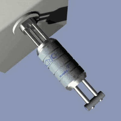
Principle of Scanning Electron Microscope (SEM)
The scanning electron microscope is a complex system that condenses electron optical technology, vacuum technology, fine mechanical structure and modern computer control technology.

The scanning electron microscope gathers the electrons emitted by the electron gun into a fine electron beam through a multi-stage electromagnetic lens under the action of accelerated high voltage.

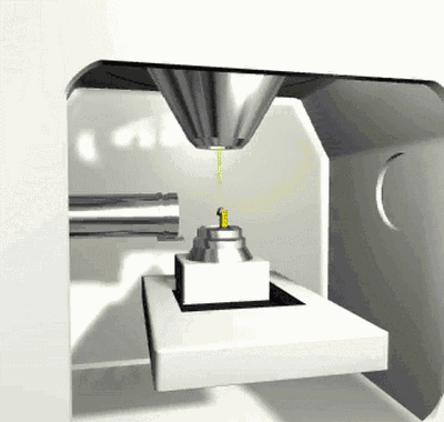
Scan the surface of the sample to stimulate various information, and analyze the surface of the sample by receiving, amplifying and displaying the information.
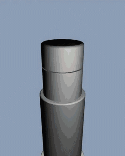
The structure of the scanning electron microscope

Structure: SEM mainly includes electron optical system, electronic system, display components and vacuum system.
Features of Scanning Electron Microscope (SEM)
- 1. High magnification, continuously adjustable between 20 times and 200,000 times;
- 2. It has a large depth of field, a large field of view, high image resolution, and a three-dimensional image. It can directly observe the fine structure of the uneven surface of various samples, and can also obtain various information corresponding to the shape;
- 3. For conductive materials, it can be directly placed in the sample chamber for analysis, and for samples with poor conductivity or insulation, a conductive layer needs to be sprayed;
- 4. The sample preparation is simple, and the original surface of the large-sized sample can be directly observed, and the pollution of the sample surface by irradiation is small;
- 5. Expand additional functions without sacrificing the characteristics of the scanning electron microscope. For example, it can be used in conjunction with EDS to analyze the composition of materials.
After we have a detailed understanding of SEM, we will then focus on its application in the field of microscopic materials and see what valuable landscapes it can present us!
Application of Scanning Electron Microscope in the Field of Metal Materials
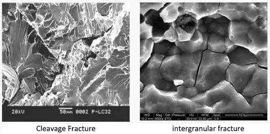
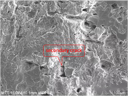
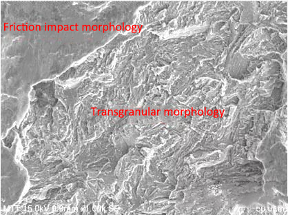
(1) Fracture failure analysis of metal materials.
Common failure forms such as wear, corrosion, fracture, and deformation exist.
Through the observation of the microscopic morphology of the fracture, according to the mechanism of brittle fracture and ductile fracture, combined with the analysis of the stress state of the material, the root cause of failure is found.
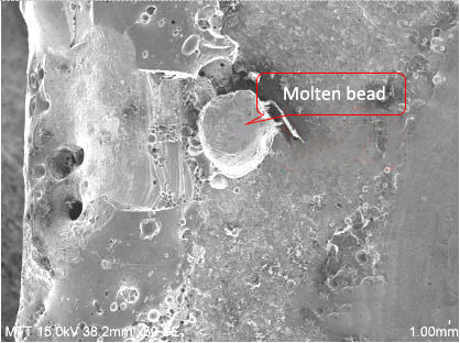
(2) Surface defect analysis of metal materials.
Common defects exist in the form of blisters, warped skins, cracks, etc.
The scanning electron microscope is used to analyze the composition, structure and energy state of the thin layer of the metal surface or interface to reveal the surface morphology, composition, structure or state of the metal material and its products.
(3) Micro-area chemical composition analysis of metal materials.
Analyze surface morphology and micro-area composition to provide qualitative and quantitative basis for inference of failure mechanism.
Determine the composition of precipitates or solid solutions in alloys, determine the segregation of various elements in metals and alloys, study the bonding state of dissimilar metals formed in electroplating and other processes, study the metal transfer phenomenon in the process of friction and wear, and the precipitation on the surface of failed parts Identification of substances or corrosion products, etc.
Application of Scanning Electron Microscope in the Field of Non-metallic Materials
(1) Observation of the surface morphology of the material
Observing the surface morphology of materials through a scanning electron microscope provides convenience for studying the morphology and structure of samples, and helps monitor product quality and improve processes.
The main content of the observation is to analyze the geometric shape of the material, the particle size of the material and the distribution of the particle size, and the structure of the phase.

(2) Analysis of coating surface morphology and measurement of coating thickness
♦Surface morphology analysis of coating
Common coating failure phenomena include: fading, blurred pattern, surface wear, corrosion, etc. Through the observation and analysis of the coating surface morphology, the product quality can be effectively controlled. The characteristics of the material section, the internal structure of the part and the morphology of the damage can all be judged and analyzed with the help of a scanning electron microscope.
♦Coating thickness measurement
The coating thickness directly affects the corrosion resistance, decorative effect, electrical conductivity, product reliability and service life of parts or products. Therefore, the coating thickness plays an important role in product quality, process control and cost control. Using a scanning electron microscope can accurately measure the thickness of the material coating, and the image is clear.
(3) Analysis of the chemical composition of the micro-area of the material
During the analysis process, after obtaining the magnified image of the morphology, it is often hoped that the in-situ chemical composition or crystal structure analysis can be performed at the same time to provide more information including the morphology, composition, crystal structure or orientation, so as to be more comprehensive and objective. judgmental analysis.
For this reason, a scanning electron microscope, a combined instrument with multiple analytical functions of an electron probe, has appeared one after another. As usual, it is used in conjunction with an EDS (X-ray energy spectrometer) to conduct qualitative and semi-quantitative analysis of materials.
(4) The resolution of the scanning electron microscope can reach the nanometer level, and it can observe nanomaterials.
All the unique properties of nanomaterials are mainly due to its ultra-fine size. By using high-resolution SEM to observe the morphology and size of nanoscale materials, it plays a fundamental role in the research and application of nanomaterials.
Practical Application Case Demonstration of Scanning Electron Microscope
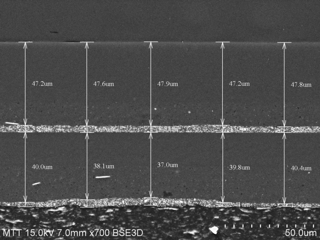
(1) For a PCB board, it is necessary to measure the thickness of the IMC layer at the specified position, and the following results are obtained.
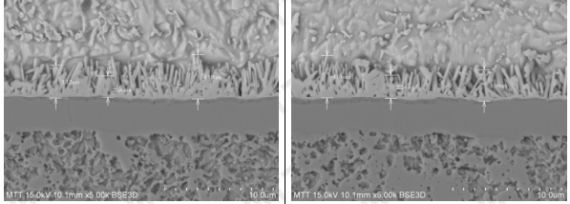
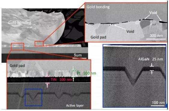
(2) Observe the internal structure of an LED chip.
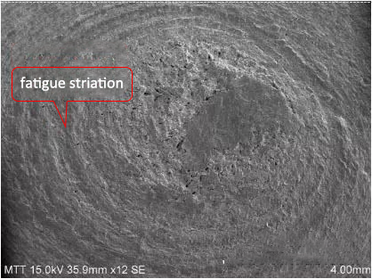
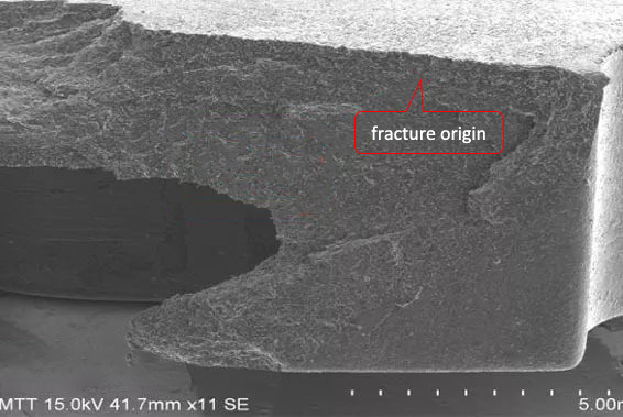
(3) Use SEM+EDS to observe the fracture position of a shaft.
Graphics observed by SEM:
Get the EDS test spectrum:
(4) A plastic part of a vehicle is fractured, and the fracture is observed by SEM.

From this, we have seen many applications of scanning electron microscopy in the microscopic field of materials, and its applications involve a wide range of industries, such as materials, electronics, aviation, automotive geology, metallurgy, machining, semiconductor manufacturing, ceramics, etc.