1. Why spray gold for non-conductive or poorly conductive samples?
Answer: SEM imaging is to obtain the signals of secondary electrons and backscattered electrons through the detector. If the sample is not conductive or the conductivity is not good, it will cause the accumulation of excess electrons or free particles on the surface of the sample and cannot be removed in time. After a certain level, charging and discharging will occur repeatedly, which will eventually affect the transmission of electronic signals and cause image distortion. Deformation, shaking and other phenomena, the conductivity of the sample surface is enhanced after gold spraying, so as to avoid the phenomenon of accumulation of electricity.
2 After spraying gold, will it affect the shape of the sample?
Answer: After spraying gold on the surface of the sample, only a few to a dozen gold atomic layers are covered on the surface, and the thickness is only a few nanometers to a dozen nanometers, which has almost no effect on the appearance.
3 What is the difference between point scan, line scan and mapping of scanning electron microscope energy spectrum?
Answer: Spectrum point scan, line scan and mapping are to obtain the semi-quantitative information of the elements of the sample in the point range, line range and surface range respectively. In addition, line scan and mapping can also analyze elements in the online or surface range of the distribution.
Their significance is that point scanning can test the type and content of elements in a certain position of the material. The significance of surface scanning (mapping) is mainly to understand the regional distribution of material elements. The significance of line scanning is to understand the element content of each point on a line of the material. Variety.
4 What are the similarities and differences between SEM and TEM?
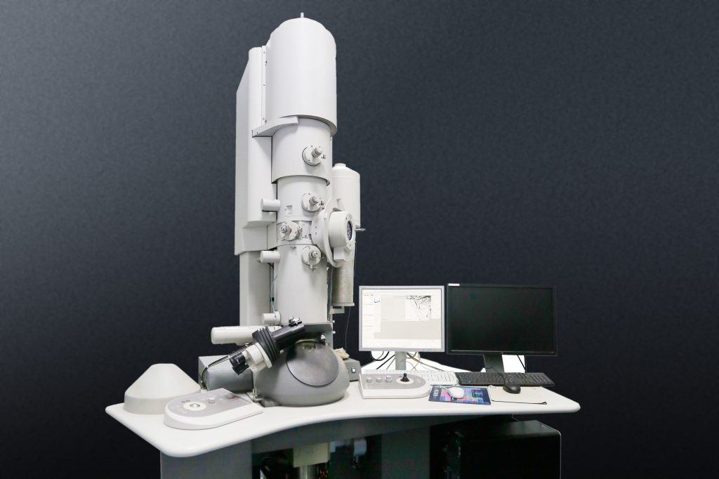
answer:
On sample preparation:
The two have common requirements for samples: solid, dry as much as possible, free from oil pollution as much as possible, and the external dimensions meet the requirements for the size of the sample chamber.
The difference is:
TEM: The penetrating ability of electrons is very weak. Transmission electron microscopy often uses high-energy electron beams of hundreds of kilovolts, but it still needs to grind samples or thin ions or ultrathin slices to micro-nano-level thicknesses. This is the most basic Require.
SEM: almost no sample preparation, direct observation. Most non-conductors need to make conductive films (such as spraying gold), and most of them can be done in a few minutes. Water-containing biological samples need to be fixed, dehydrated and dried.
On imaging:
During SEM imaging, the electron beam does not penetrate the sample but scans the surface of the sample. During TEM imaging, the electron beam penetrates the sample. The spatial resolution of SEM is generally XY-3-6nm, and the spatial resolution of TEM can generally reach 0.1-0.5nm.
5 What is the difference in sampling depth between SEM-EDS and XPS tests?
Answer:
The sampling depth of XPS is 2-10nm, and the sampling depth of EDS is about 1um.
6 Why can’t the energy spectrum of the scanning electron microscope be accurately quantified?
Answer:
Energy Spectroscopy (EDS) combined with scanning electron microscopy can analyze the type and content of elements in the micro-area of materials.
Its working principle is: each element has its own X-ray characteristic wavelength, and the size of the characteristic wavelength depends on the characteristic energy E released during the energy level transition. The energy spectrometer uses the characteristic of different X-ray photon characteristic energies of different elements to analyze the composition. The accuracy of energy spectrum quantitative analysis is related to the sample preparation process, the conductivity of the sample, the content of elements and the atomic number of elements.
Therefore, in the process of quantitative analysis, there are not only some theoretical errors (database and standards), which we cannot eliminate, but also some errors caused by human factors. These elements will lead to inaccurate quantification of energy spectra.
7 What is a backscattered electron image?
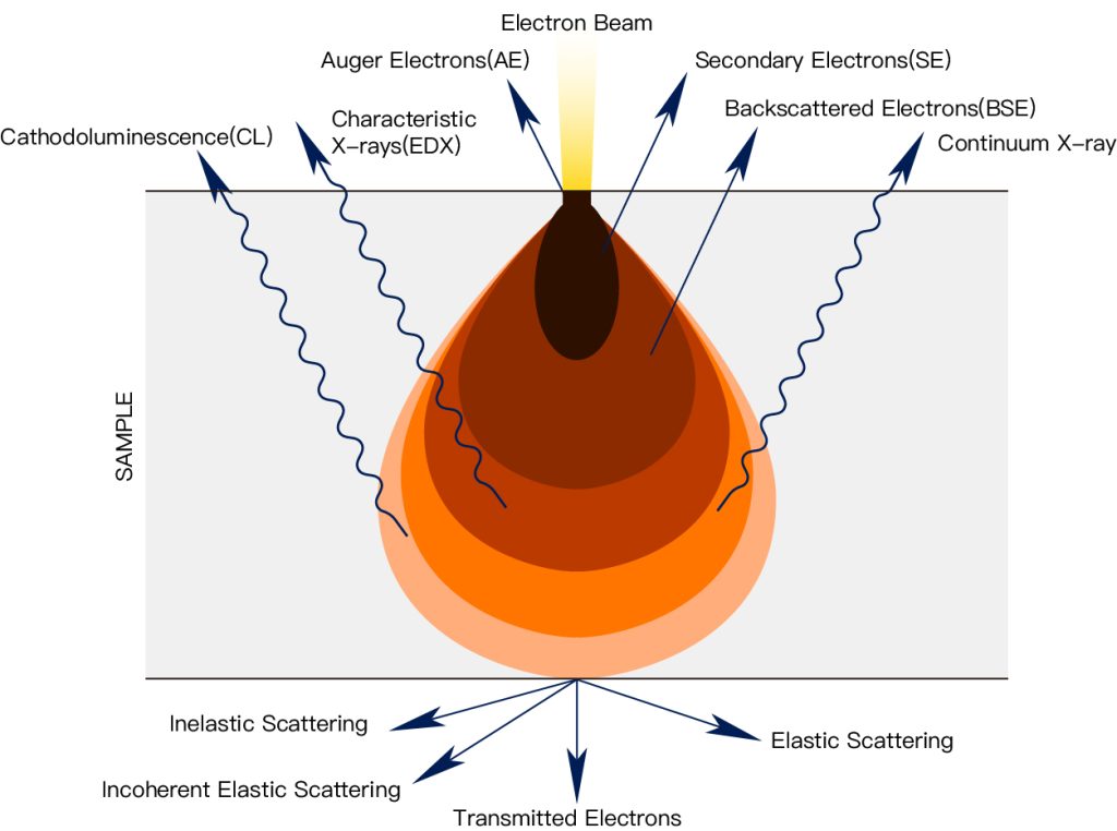
Answer:
Backscattered electrons (Backscattered Electrons): The incident electrons are scattered in the sample and then emitted from the upper surface. It reflects the regional differences of different orientations and different average atomic weights on the sample surface.
The formation of the backscattered electron image is due to the formation of a brighter area on the surface of the sample with a larger average atomic number, which produces a stronger backscattered electron signal; while a lower average atomic number produces less backscattered electrons. Electrons are the darker areas on a fluorescent screen or in a photo, thus creating atomic number contrast.
8 What is the relationship between the scale of the electron microscope image and the magnification?
Answer:
The scale of the electron microscope image can usually be set to be fixed or variable. The former means that the length of the scale remains constant, but the representative length changes with the magnification; the latter means that the length of the scale adapts to the variable magnification at different stages, but the representative length is fixed within a certain magnification range.
So the same magnification can have different scales, but the actual size on the same output medium remains the same. When changing the output mode, the magnification has changed (of course the displayed magnification will not change), and of course the measured size will also change.
Therefore, the value of the scale has no necessary relationship with the magnification, and the specific value is related to the settings of different instrument manufacturers.
9 Is the topography shooting result not clear?
answer:
- The conductivity of the sample is poor, resulting in unclear shooting results;
- The shooting requirements are too high for the instrument itself to meet;
- The focus or astigmatism is not adjusted properly, which is generally rare;
- Secondly, it also has a certain relationship with the equipment configuration and installation environment.
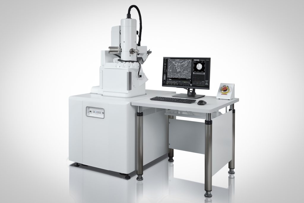
10 What are the classifications of scanning electron microscopes?
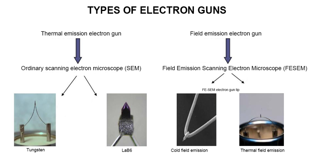
Answer:
Scanning electron microscopes can be divided into thermal electron emission type and field emission type according to the different ways of generating electrons. The filaments used in thermal electron emission type mainly include tungsten filament electron microscopes; field emission types are divided into thermal field emission and cold field emission.