A scanning electron microscope (SEM) uses a highly concentrated high-energy electron beam deflected by an electromagnetic lens to bombard the surface of the sample, and the secondary electrons, backscattered electrons, etc. or fracture morphology for observation and analysis.

SEM has the characteristics of large depth of field, high resolution, intuitive imaging, strong stereoscopic effect, wide magnification range, and the sample to be tested can be rotated and tilted in three-dimensional space. It is currently widely used in nanotechnology, metals, semiconductors, ceramics and fields of medical biology.
How Scanning Electron Microscopes (SEM) Work
When the top electron light source (usually called an electron gun) irradiates the sample surface, about 90% of the energy is converted into heat energy, and the remaining energy generates a series of information: such as secondary electrons, Auger electrons, backscattered electrons, X-rays, cathode fluorescence , electron-hole pairs and absorbed current, etc., and transmitted electrons for thin film samples.
Due to the different situations in which the incident electrons of the probe interact with the sample atoms and the physical mechanism for generating a series of information itself, the depth of a series of information generated in the sample is also different, and the characteristics and collection methods of various information are also different.
If the electronic probe is used for raster scanning, a certain kind of information generated will be collected point by point with the corresponding detector, after proper processing and amplification, and the brightness of the synchronous scanning picture tube will be modulated with this signal, A sample image of this information can be obtained on the fluorescent screen of the kinescope.
(1) scan
When the high-energy electron beam generated by the electron gun is incident on a certain part of the sample, elastic scattering and inelastic scattering events occur in the interaction area, resulting in backscattered electrons, secondary electrons, absorbed electrons, characteristic and continuum X-rays, Russian Various useful signals such as intermittent electrons and cathodofluorescence can be detected by using suitable detectors to determine certain properties of the sample in the electron incident site, such as micro-domain morphology or composition. In order to study the characteristics of more parts on the sample, the scanning system must be used to move the incident electrons to different positions on the sample.
(2) Imaging
The imaging of the scanning electron microscope is realized by scanning. The scan generator simultaneously controls the “synchronous scanning” of the high-energy electron beam and the electron beam in the fluorescent screen. When the electron beam performs grid scanning on the sample, it also scans synchronously on the fluorescent screen in the same way, so a “sample space” The series points correspond to the “display space” point by point.
In other words, each position of the electron beam on the sample has a strict correspondence with each point on the fluorescent screen. The surface of the sample is scanned by the electron beam to excite various physical signals whose intensity is related to the surface characteristics of the sample. These signals are sequentially and proportionally converted into video signals through the detector, and after amplification, they are used to modulate the electrons at the corresponding points of the fluorescent screen. The beam intensity, that is, the brightness of the spot, forms the image of the SEM.
The change in intensity on the image reflects the properties of the sample. Although the scanning electron microscope imaging is not directly imaged by the light or electron beam emitted by the object like the light microscope and the transmission electron microscope, this imaging process is like using the signal detector as a camera to shoot the sample surface point by point, and convert the signal generated by each point to the fluorescent screen. on the imaging.
The image on the fluorescent screen is actually composed of a series of bright spots with different gray levels, which are called pixels (Pixle). The more pixels, the higher the resolution of the image.

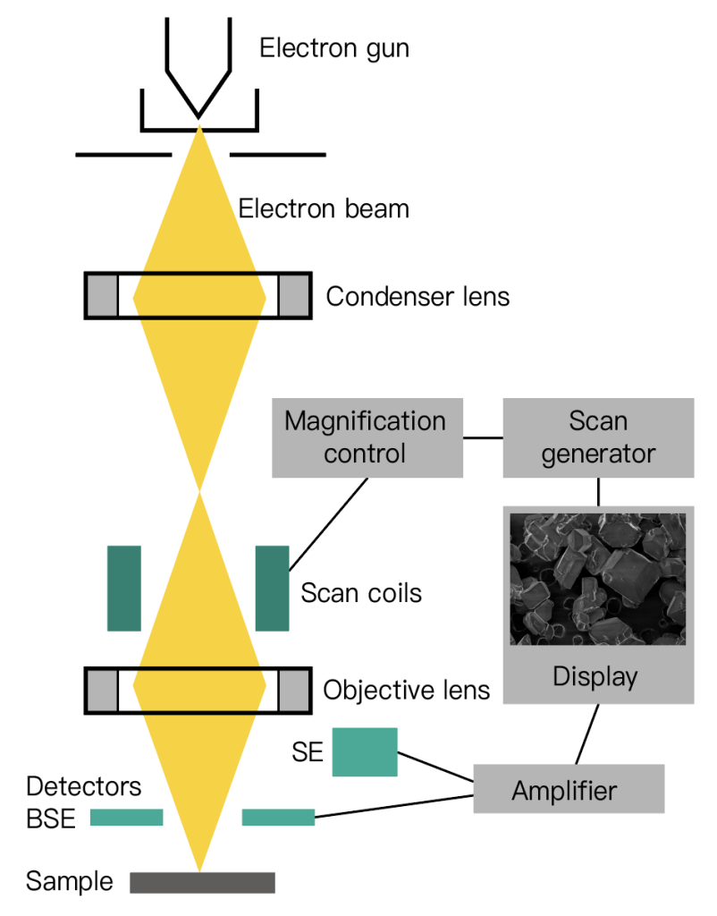

Schematic diagram of SEM working principle
Sample Preparation
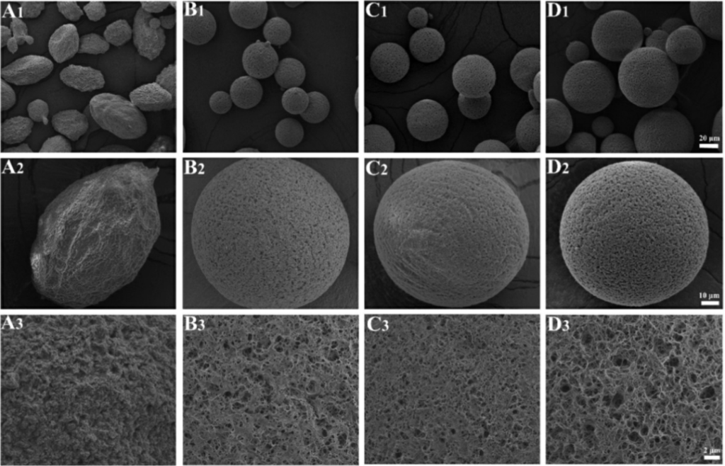
1. When using SEM to observe biological samples, such as animal body fluids, muscles, hair and some tissues and organs, as well as various microorganisms (bacteria, fungi, etc.), the sample preparation step plays a vital role in the imaging quality.
2. The water content of biological samples is high, generally 70%-80%. Most biological samples need to be dehydrated and dried before they can be observed. Only a few samples, such as some pollen, hair, etc., can be directly put into the scanning electron microscope for observation.
3. For the sample preparation steps of cells, tissues and bacteria, please refer to the document Sample Preparation Guide.
4. It is forbidden to use the scanning electron microscope to observe wet or volatile samples, which will cause a sharp drop in the vacuum in the chamber, resulting in image drift, white streaks, and will affect the life of the filament and cause permanent damage to the instrument.
5. After the sample is fixed on the sample table and before entering the sample chamber after spraying gold, it needs to be purged with a dust removal tank. On the one hand, it is to avoid the floating dust in the environment from interfering with the observation of the sample. Firm particles, avoid being sucked in and damage the equipment when vacuuming.
Naturally dried mouse tracheal villi (left picture) and critical point dry tracheal villi (right picture) | Source: PHENOM SCIENTIFIC official website
Spray gold
In most cases, no matter what sample preparation, SEM can theoretically provide nanoscale information of various samples. In some cases, in order to obtain better SEM images, the SEM can be used in combination with a gold sprayer (ion sputterer).
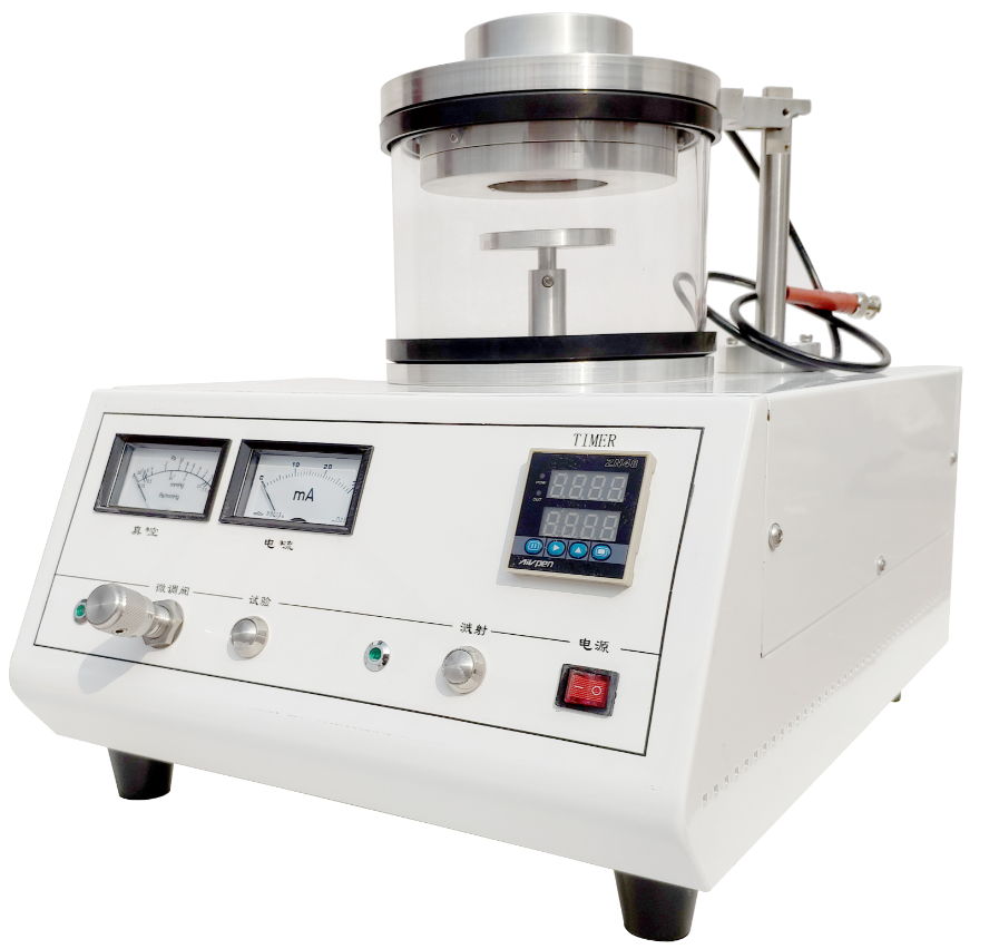
Due to the excellent high conductivity of gold, the sample material sprayed with gold by sputtering can increase the signal-to-noise ratio during scanning electron microscopy imaging, thereby improving the quality and resolution of the image. However, it should be noted that after spraying gold, the surface is no longer the original material, and the contrast information of the elements will be lost.
system operation
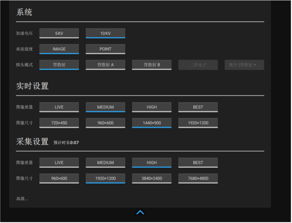
Selection of Accelerating Voltage
When the accelerating voltage is small, the energy of the incident electron beam is low, the depth of interaction between the electron beam and the sample is small, the difference between light and dark is reduced, the image appears relatively soft, and the surface details of the bright and dark areas can be observed well, but the image is three-dimensional. Not feeling enough.
When the accelerating voltage is high, the energy of the incident electron beam is high, the depth of interaction between the electron beam and the sample is large, and the difference in brightness and darkness will be large, and the raised tip will appear extremely bright. Although the image has a strong three-dimensional effect, it is not soft.
Beam intensity
There are two options for beam intensity, IMAGE and POINT. POINT is generally used as the beam spot size used in spectral point analysis to ensure sufficient signal-to-noise ratio.
Note: The scanning electron microscope at the center is currently not equipped with an energy dispersive spectrometer.
Probe mode
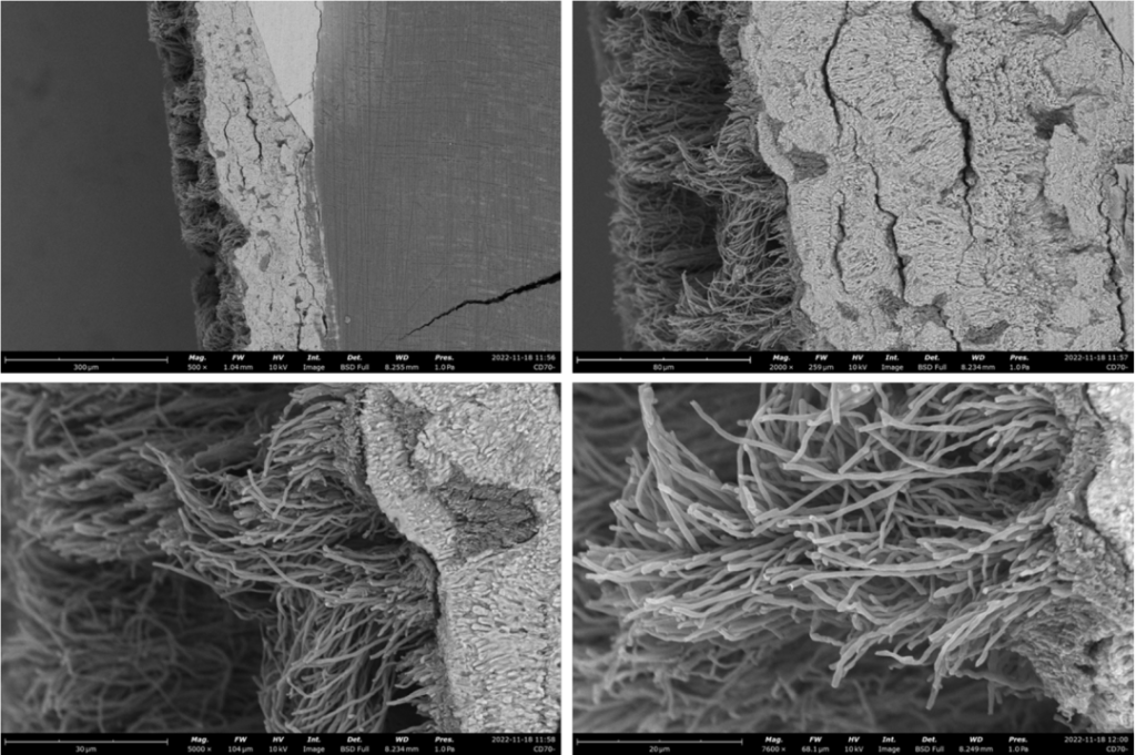
The secondary electron image mainly reflects the morphology of the sample.
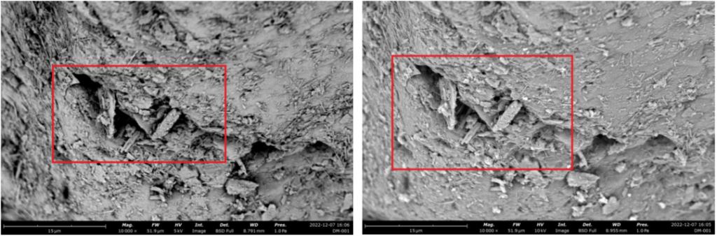
The backscattered electron image not only reflects the sample morphology, but also reflects the chemical composition information of the sample. According to the relationship between backscattered electrons and atomic number, generally speaking, the region with higher brightness is composed of components with larger atomic number, and the region with lower brightness is composed of components with small atomic number.
When using a scanning electron microscope to observe a sample, you can choose a suitable mode according to the purpose of the test. For example, when testing the surface morphology and fracture analysis of powder samples, since the surface of this type of sample has large fluctuations, the secondary electron mode can be used at this time to obtain good shooting results.
When performing tests such as foreign matter analysis and cross-sectional size measurement, by using the backscattered electron mode to shoot, you can observe obvious color contrast and clearly observe the images of different components.
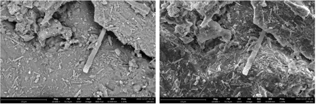
Image display
Plaque and calculus on the surface of teeth | Source: Department of Stomatology, The Fifth Affiliated Hospital of Sun Yat-sen University