Ferroelectric ceramics are ceramic materials with ferroelectric properties, constituting an important branch within ceramic materials. The specific manifestation of ferroelectricity involves the spontaneous parallel arrangement of electric dipoles due to dipole-dipole interactions, akin to ferromagnetism. Below a certain temperature, the disorderly arrangement of dipoles caused by thermal energy is overcome by a local electric field, resulting in spontaneous polarization, where all electric dipoles align in a parallel array.
Ferroelectric ceramics exhibit high dielectric constants below the Curie temperature, allowing electric dipoles to spontaneously polarize the material, and the direction of spontaneous polarization can be altered with an external field. The higher the dielectric constant, the stronger the binding or storage capacity of charges, indicating better insulation properties of the material. Common ferroelectric materials include barium titanate, lead titanate, potassium dihydrogen phosphate, and Rochelle salt, among others.
Ferroelectric Ceramic – Barium Titanate (BaTiO3)
Barium titanate, or its solid solution, is the main crystalline phase in ceramics, synthesized primarily from barium carbonate and titanium dioxide. Its crystal structure comprises barium ions and oxygen ions forming a face-centered cubic lattice, with titanium ions situated at the octahedral oxygen centers. Barium titanate exhibits a perovskite-type structure (ABO3) and is a typical ferroelectric material, with a Curie temperature of approximately 125°C.
Barium titanate is a key raw material in the production of electronic ceramics, often referred to as the “pillar of the electronic ceramics industry.” It is used as a dielectric material in the preparation of multilayer ceramic capacitors (MLCC).
As a ferroelectric material, barium titanate possesses high dielectric constant and low dielectric loss characteristics, along with excellent ferroelectric, piezoelectric, pressure-resistant, and insulating properties. It finds widespread applications in manufacturing ceramic sensing components. High-purity, nanoscale barium titanate has gradually become the mainstream product in the market.
High purity is a stringent requirement to ensure the reliability and stability of downstream products. Nanoscale barium titanate powders, after sintering, result in denser texture, more uniform particle size distribution, and enhanced ceramic toughness, and strength. Additionally, nanoscale powder requires lower sintering temperatures, contributing to energy savings and reduced production costs. The preparation process of high-purity barium titanate powder is crucial to meet the requirements of the electronic ceramics industry.
Microstructure, product performance, and production process conditions in ceramic production are closely interrelated. Analyzing the microstructure of ceramic powders can infer variations in process conditions and reflect the quality of materials. SEM analysis of powder material defects can quickly identify the causes of defects.
Due to the poor conductivity of barium titanate, the sample surface accumulates charges under the action of high-energy electron beams in SEM, causing electron beam deflection and hindering the display of the sample surface’s true morphology. Therefore, in SEM sample preparation, the sample needs to undergo conductive treatment.
Scanning Electron Microscopy of Barium Titanate Powder
Field Emission Gun Scanning Electron Microscope (FEG-SEM) is a high-resolution electron microscope primarily used for high-definition imaging and analysis of sample surfaces. It employs a field emission gun as the electron source, providing a more intense and stable electron beam compared to traditional thermionic cathode electron sources, thus achieving higher resolution.

Key features and principles of Field Emission Gun Scanning Electron Microscope:
- Field Emission Gun: The electron microscope uses a field emission gun as the electron emission source. The working principle involves applying a strong electric field at the tip to emit electrons. This results in a higher brightness and more stable electron beam compared to traditional thermionic cathode emission sources.
- High Resolution: FEG-SEM achieves very high spatial resolution due to the field emission gun. This allows for a clearer display of the microstructure of the sample surface, enabling scientists and researchers to observe smaller details.
- Scanning Electron Microscope: FEG-SEM is a type of scanning electron microscope that, unlike traditional transmission electron microscopes, can not only observe surface morphology but also obtain information on the chemical composition of the sample surface. By scanning the sample surface and measuring reflected and scattered electrons, high-resolution images can be generated.
Application fields of field emission gun scanning electron microscope
Application Areas: FEG-SEM is widely used in materials science, biology, nanotechnology, and other fields. In materials science, it is used to study the microstructure of metals, ceramics, polymers, and other materials. In biology, it can be used to observe the microstructure of cells, tissues, and other biological samples.
In summary, Field Emission Gun Scanning Electron Microscope is an advanced electron microscope that employs advanced field emission technology and the principles of scanning electron microscopy to provide high-resolution surface imaging and analysis for scientific research.
Field Emission Gun Scanning Electron Microscope can meet most samples’ microscopic morphology testing requirements, providing excellent imaging effects. It supports using multiple hardware devices, and most functions can be automated. It features a low vacuum mode with continuously adjustable vacuum levels from 10 to 270 Pa, suitable for imaging sensitive and biological samples. The use of scanning electron microscopy allows for the intuitive and accurate observation of the distribution, particle size, and morphology of powder samples. For nanoscale powder particles, the use of Field Emission Gun Scanning Electron Microscope allows for detailed observations at magnifications of up to one hundred thousand times.
The following sets of observation images are captured using the Field Emission Gun Scanning Electron Microscope and conventional scanning electron microscopy, displaying images of barium titanate powder.
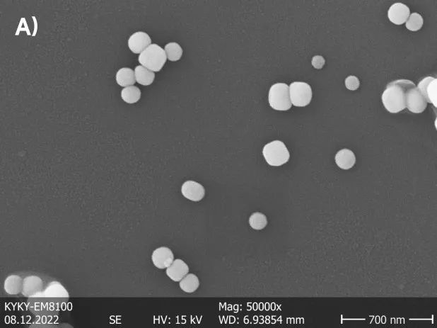
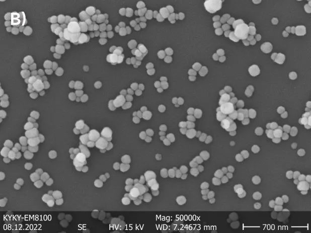
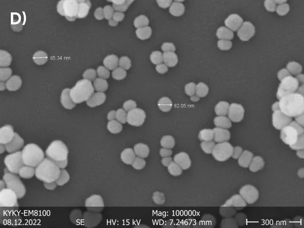
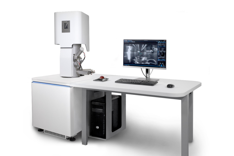
Image 1 shows two types of nanoscale barium titanate powders with different particle sizes. Differences in particle sizes are evident within their respective systems. From a morphological perspective, the sample with a larger particle size exhibits a smooth and regular edge, while the sample with a smaller particle size appears irregular and prone to stacking.
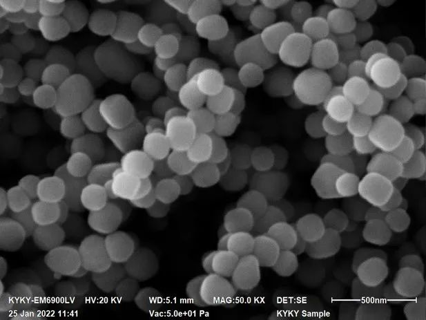
Image 2 displays barium titanate powder directly adhered to a conductive adhesive tape, revealing significant particle aggregation and overlap due to the friction-generated charges during the grinding process.
The preparation of samples directly affects the imaging quality of SEM. Friction-generated charges during grinding can lead to particle accumulation and instability, resulting in particle aggregation during adhesion to the conductive adhesive tape. To observe single-layer powder particles or even individual particles, the sample undergoes pre-treatment.
Firstly, a small amount of powder is dispersed in anhydrous ethanol (the choice of dispersion medium depends on the polarity of the solute and solvent, selected according to the principle of similar solubility), uniformly sonicated, and then dropped onto a silicon wafer (one drop is sufficient; excessive drops can lead to stacking). After drying in an oven, gold coating is applied. For samples with uncertain concentration suitability, samples with 3-5 concentration gradients are prepared for testing to identify the concentration that ensures uniform sample distribution. This method significantly improves the phenomenon of aggregation, providing clear basal observation and facilitating imaging, as shown in Image 1.