The TEM market is a dynamic and rapidly evolving industry with a quick pace of introducing new products and technologies.
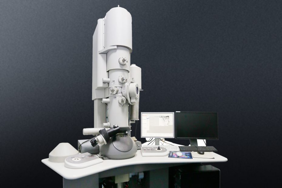
TEM is an imaging technique where an electron beam passes through an extremely thin sliced specimen. When electrons transmit through the sample and interact with its structure, the image is magnified and focused onto an imaging medium (such as photographic film or a fluorescent screen) or captured by a specialized CCD camera.
Due to the very small wavelength of electrons used in TEM, it can achieve higher-resolution imaging compared to traditional optical microscopes that rely on light beams. With its higher resolution, TEM plays a significant role in virology, cancer research, materials research, and microelectronics development.
Limitations of Transmission Electron Microscopy
TEM is an important technique that has entered the field of cell biology. Compared to optical microscopes, TEM can achieve very high resolution due to the shorter wavelength of the electron beam. This capability allows TEM to visualize cellular structures such as membrane systems, cilia, organelles, and their complexities. However, TEM also has its own limitations.
Sampling Capability:
Every high-resolution imaging technique has its limitations: at any given time, only a small portion of a sample can be examined, and the higher the resolution, the lower the sampling capability. So far, all TEM has only been used for analyzing sample materials. Researchers must understand the basic aspects of the sample before attempting to investigate finer details.
Projection Limitation:
The working principle of TEM allows us to see 2D images of 3D specimens as a transmission part. Since our eyes and brain typically understand reflected light, we may assume that we can interpret TEM images, but this is not the case.
For example, when we see a picture of two animals with their backs to each other, it may (in 2D) appear as a single body with two heads on each end, but we still understand the true nature of the animals in a 3D scene. In contrast, when we see similar misleading TEM images, we may not be able to interpret them correctly, and artifacts may also exist in TEM images.
This particular flaw in TEM is known as the projection limitation. One specific aspect of this limitation is that the images, diffraction patterns, or spectral information obtained through TEM are averaged over the thickness of the sample. This means there is no depth sensitivity in a single TEM image.
The thickness of the sample is undoubtedly known, but it is not immediately visible. Therefore, it is necessary to utilize other surface-sensitive or depth-sensitive techniques, such as scanning probe microscopy, field ion microscopy, Rutherford backscattering, and Auger spectroscopy, as complementary techniques to completely characterize the sample.
Biophysicists have invented electron tomography, a technique that creates 3D images using a large number of images taken from different angles, similar to the use of X-rays in modern medical CAT (computed axial tomography) scans. Sample holders have been continuously improved to enable 360-degree rotation. This, along with data storage and manipulation, helps nanotechnologists study complex inorganic structures (e.g., porous materials) containing molecules of interest (e.g., catalysts).
Damage from Radiation:
Ionizing radiation always damages the samples used in TEM. Examples of materials that can be damaged by ionizing radiation include polymers, organic materials, certain minerals, and ceramics. This damage worsens at voltages as high as 400 kV, which is achievable in many commercial instruments. However, with the advancement of technology, the combination of high electron beams, sensitive electron detectors, and computer enhancement of noisy images is achieved in such a way that the total dose received by the sample is below the damage threshold. This method, known as minimal dose microscopy, is often combined with sample cooling (cryo-electron microscopy) and low-noise CCD (charge-coupled device) cameras, which have become standard techniques in biological TEM research.
Despite all the progress, the combination of high electron beams and strong electron sources can damage any type of sample/tissue. It can also potentially expose oneself to harmful radiation. Although modern TEM designs prioritize safety, it is important not to modify the instrument in any way without consulting the manufacturer and without performing all routine radiation leakage tests.
- Sample Preparation:
TEM is based on the principle of transmitting electrons to obtain information about the sample. The sample needs to be thin – the material must be electron-transparent. This means that the electrons passing through the material and landing on the screen or film must have sufficient intensity to generate an image within a reasonable time frame. This is typically a function of the electron energy and the average atomic number (Z) of the observed sample.
Thinner specimens are preferred; it is recommended to use samples smaller than 100 nm. For high-resolution TEM or electron spectroscopy, sample thickness less than 50 nm (or even less than 10 nm) is common. However, as the beam voltage increases, these limitations may not apply, which can lead to sample damage and artifact generation.
It is recommended to study the material at low magnification using the naked eye, visible scanning electron microscope, and optical microscope before attempting to use TEM for material research. Failure to follow this general approach can easily lead to misinterpretation of artifacts that may arise in TEM methods.
Trends in the Development of Transmission Electron Microscopy
The development trends of transmission electron microscopy (TEM) encompass several aspects as follows:
- Improved resolution: Enhancing resolution has always been a primary goal in TEM development. High-resolution TEM has already achieved resolutions below 0.5Å. Advancements in next-generation monochromators and aberration correctors further enhance the energy and spatial resolution of TEM. Particularly in low-voltage electron microscopy, atomic structures and crystal defects can be observed with greater clarity.
- Multidimensional imaging techniques: Presently, TEM can accomplish multidimensional imaging, such as High-Angle Annular Dark-Field (HAADF) imaging and tomography. These techniques will continue to be refined and developed in the future to enable more comprehensive observations of sample structures and compositions.
- Data analysis and image processing techniques: With the continuous advancement of computer technology, the amount of data generated from TEM imaging is increasing. Consequently, data analysis and image processing techniques are becoming increasingly important. Ongoing research and development in these areas aim to accurately analyze and interpret information within TEM images.
- Multifunctionality: Future TEM instruments will gradually become more multifunctional, combining transmission electron microscopy with scanning electron microscopy, as well as integrating with other techniques such as spectroscopy and atomic force microscopy. This integration aims to provide a more comprehensive understanding of material properties and structures.
Summy
Since the inception of TEM over 80 years ago, it has played a crucial role in resolving numerous scientific challenges. TEM continues to advance with increased functionality and improved performance. Although there are still challenges and issues to address, the future development of TEM will focus on high resolution, multidimensional imaging, data analysis and image processing techniques, and multi-functionality.