Failure analysis is a developing emerging discipline that has been popularized from the military industry to ordinary enterprises in recent years. It generally involves analyzing and verifying failure modes and phenomena, simulating and reproducing the phenomenon of failure, identifying the cause of failure, and excavating the mechanism of failure.
It has strong practical significance in improving product quality, technological development, improvement, product repair, and arbitration of failure accidents.
What is failure analysis?
The so-called failure analysis is based on failure phenomena, through information collection, visual inspection, and electrical performance testing, to determine the failure location and possible failure modes, namely failure localization;
Then, for the failure mode, a series of analysis methods are adopted to conduct cause analysis and root cause verification;
Finally, based on the test data obtained during the analysis process, prepare an analysis report and propose improvement suggestions.
Scanning electron microscopy is widely used to predict the morphology, structure, interface condition, damage mechanism, and material performance of various materials. It can directly observe the aggregation mode and true boundaries of atoms inside materials, study crystal defects, and analyze the failure principle.
Definition and Principle
Scanning electron microscopy involves electronic optics technology, vacuum technology, fine mechanical structure, and computer control technology, and is a complex system combination. It uses an electron beam to scan the sample, while using a detector to receive various signals excited by the electron beam on the sample, and uses a signal detection and amplification system to output modulated signals for conversion. The image is now generated in the display system.
These signals mainly contain secondary electrons for morphology observation; Backscattered electrons, characteristic X-rays, and Auger electrons, used for composition analysis.
In failure analysis, SEM has a wide range of application scenarios, playing a crucial role in determining failure analysis modes and identifying failure causes.
The focal depth of a scanning electron microscope is 10 times larger than that of a transmission electron microscope and several hundred times larger than that of an optical microscope. Due to the large depth of field in the image, the scanned electronic image is three-dimensional and has a three-dimensional shape. Compared to other microscopes, it can provide more information.
Composition of electron microscopy
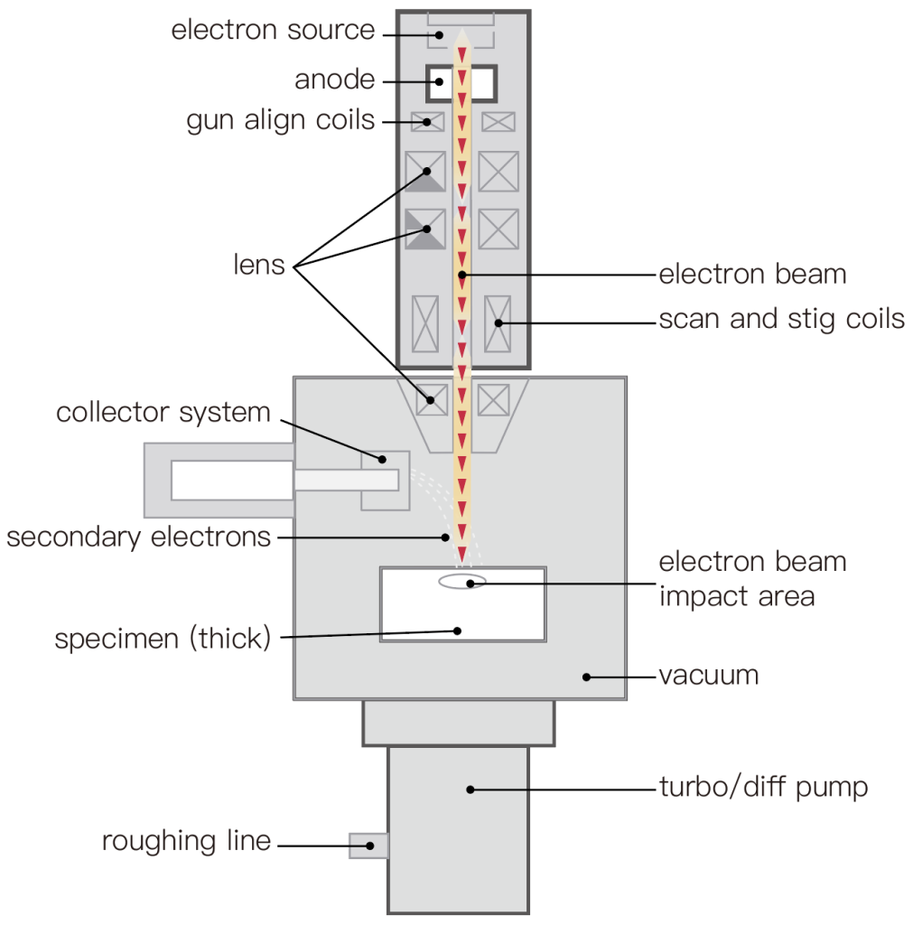
The main four systems are electronic optical systems, signal collection and display systems, vacuum systems, and power supply systems.
(1) Electronic optical system: mainly includes components such as electron guns, electromagnetic lenses, scanning coils, and sample chambers.
Electromagnetic lens: Focusing on the beam spot of the electron gun, the smaller the beam spot, the smaller the imaging unit, and the higher the resolution.
Scanning coil: deflects the electron beam and performs a grating like scan on the sample to excite various electronic signals.
Sample room: Place samples and install various signal detectors.
(2) Signal collection and display system: Collect various signals generated by the sample under the action of an incident electron beam, such as secondary electrons, backscattered electrons, characteristic X-rays, etc., and perform amplification and conversion to display the image on the display system.
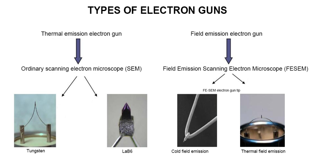
(3) Vacuum system: The electron gun of a field emission electron microscope requires high vacuum, so it is equipped with two ion pumps, one molecular pump, and one mechanical vacuum pump.
(4) Power system: including various power sources for startup, detection amplification system, vacuum system, and imaging system.
Electronic signal
Secondary electrons (SEI) refer to extranuclear electrons that are bombarded by incident electrons. It mainly comes from a shallow area less than 10nm from the surface, which can effectively display the micromorphology of the sample surface and has little correlation with atomic number. It is generally used to characterize the surface morphology of the sample.
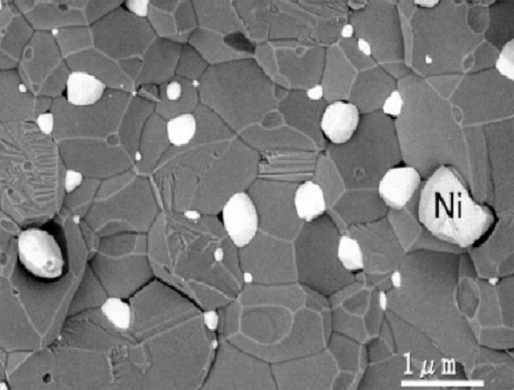
Backscattered electrons (BEI) refer to high-energy electrons that escape from the surface of the sample after the interaction between the incident electrons and the sample. Compared to secondary electrons, backscattered electrons are positively correlated with the atomic number of the sample, and the depth of collection is deeper, mainly used to reflect the elemental characteristics of the sample.
Comparison of SEI and BEI images
SEI
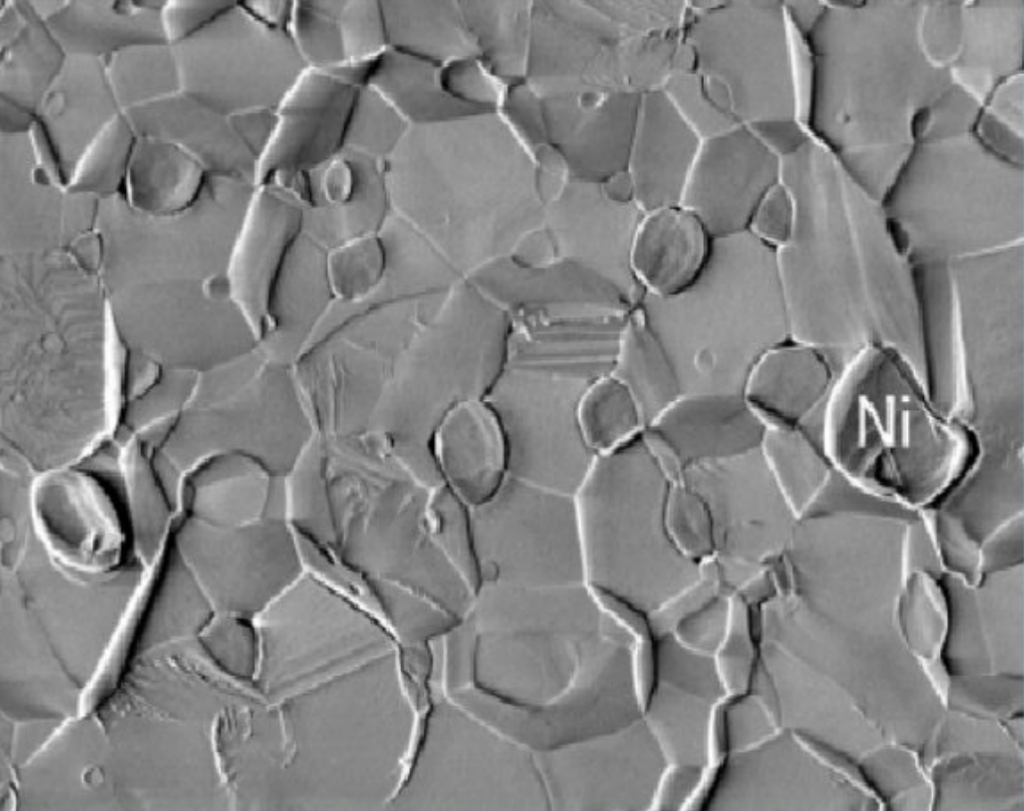
BEI
Sample preparation
The sample preparation technology is related to the observation effect of electron microscopy images and the correct interpretation of images. There are certain requirements for the conductivity of the sample, and the accumulation and discharge of generated charges can cause unclear images or make it difficult to observe and take photos.
Requirements for conventional electron microscope samples: they must be dry and free from moisture or volatile substances; Has a certain mechanical strength and can withstand electron beam bombardment; It has conductivity and can generate sufficient secondary electrons when excited.
- Preparation of block samples
For block shaped conductive samples, there is basically no need to prepare them. As long as their size is suitable for the size of the electron microscope sample base, the sample can be directly bonded to the sample base using conductive tape and observed in a scanning electron microscope. To prevent the existence of artifacts, the sample should be cleaned with acetone or alcohol before being placed, and if necessary, cleaned with an ultrasonic cleaner. For bulk non-conductive samples or samples with poor conductivity, coating treatment should be carried out first. Otherwise, the surface of the sample will generate charge accumulation under the action of high-strength electron beams, affecting the motion trajectory of the incident electron beam spot and the secondary electron emitted by the sample, resulting in a decrease in image quality. Therefore, such samples should be sprayed with a conductive layer before observation, forming a conductive film on the material surface to avoid charge accumulation on the sample surface, Improve image quality and prevent thermal damage to the sample.
- Preparation of powder samples
For conductive powder samples, the conductive tape should be bonded to the sample holder first, and then the powder sample should be evenly spread on top. The unbound powder should be blown away with an ear wash ball, and then observed using an electron microscope. For non-conductive or poorly conductive materials, an additional layer of conductive film should be coated before electron microscopy can be used for observation. In order to accelerate the testing speed, multiple samples can be prepared simultaneously on a sample holder, but when using ear wash balls to blow unbound powder, care should be taken not to contaminate each other between the samples.
For the preparation of powder samples, the following points should be noted:
A. Try not to squeeze the sample as much as possible to maintain its natural morphology.
B. Fine and small samples can be dispersed in ethanol or a suitable solvent using ultrasound, and then dropped onto the conductive tape on the sample stage using a capillary tube (or a toothpick can be used to drop onto the sample stage). They can be dried or dried under strong light before opening.
C. The thickness of the powder sample should be uniform, the surface should be flat, and the amount should not be too much, about 1g, otherwise it is easy to cause the powder to peel off the surface during observation, or it is easy to cause poor conductivity of the bottom layer of the gold sprayed sample, resulting in poor contrast of the observation effect.
- Semiconductor materials
General sample preparation methods are suitable. But some special contrast mechanisms, such as voltage contrast, electron channel contrast, induced current, sample current, etc., require special preparation of semiconductor materials.
- Metal and ceramic samples
Thoroughly remove oil stains to avoid hydrocarbon contamination. Ultrasonic cleaning machine: solvents include acetone, ethanol, toluene, etc. It is very important that the solvent does not harm the surface morphology integrity of the sample.
Method for determining sample contamination: Observe the sample at high magnification, then reduce the magnification (scanning electron microscopy is a confocal system, with clear focus at high magnification and no defocusing at low magnification). If there is contamination, obvious black marks will be observed in the original high-magnification scanning area at low magnification. The rate of pollutant deposition is related to the dose in the electron beam irradiation area. The higher magnification, the higher the electron beam irradiation dose per unit area of the sample during the same scanning time.
For non-metallic materials with poor conductivity, conductive films such as C, Au, Pt must be evaporated. Quantitative analysis of C plating, the morphology of Au and Pt plating; The surface of the sample should not be contaminated and should be cleaned when appropriate; Magnetic samples must undergo special treatment.
Practical Applications and Cases
The main application scenarios of SEM in failure analysis:
Surface morphology observation (foreign objects)
Cross-section observation (IMC, phosphorus-rich layer, etc.)
Fracture analysis (analysis of metal fracture surface texture)
Summary
From the above, it can be seen that the results of SEM analysis are an important basis for failure judgment throughout the entire failure analysis process. Based on this, the next step of analysis and inference is made to assist in finding targeted improvement or preventive measures for failure analysis work, ultimately forming a closed loop during the failure analysis process.
Field emission scanning electron microscope SEM4000
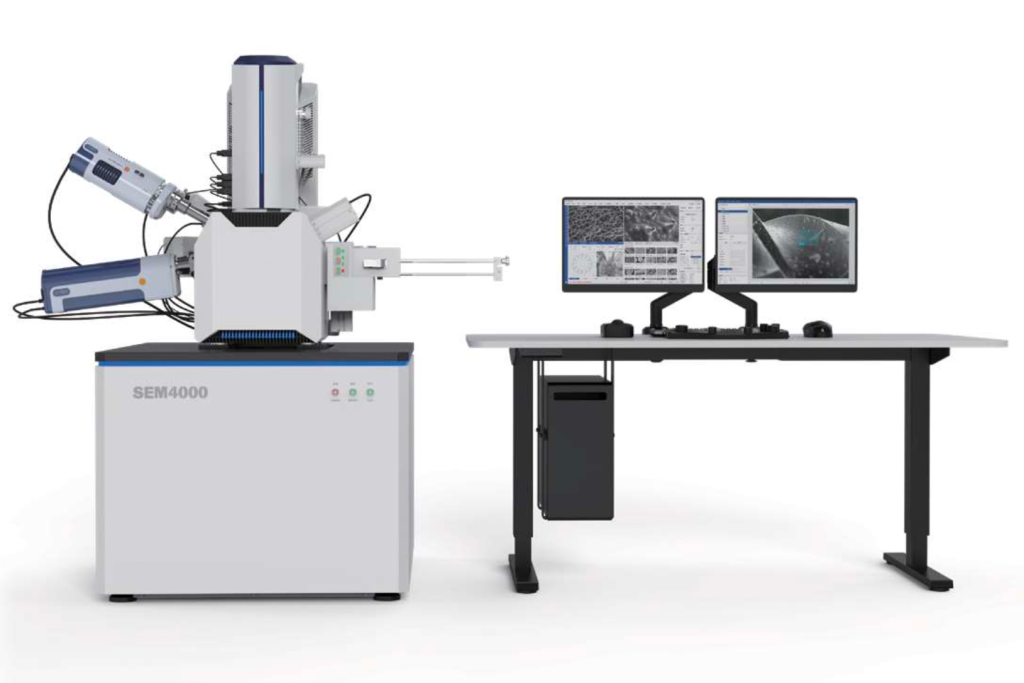
SEM4000 is an analytical thermal field emission scanning electron microscope equipped with a high-brightness, long-life Schottky field emission electron gun. The three-stage magnetic lens design, with a beam current up to 200 nA and continuous adjustable, has obvious advantages in EDS, EBSD, WDS and other applications. Support low vacuum mode, can directly observe the conductivity of weak or non-conductive samples. Standard optical navigation mode, as well as intuitive operation interface, make your analysis work feel more relaxed.