Ceramic materials have a series of characteristics such as high melting point, high hardness, high wear resistance, and oxidation resistance, and are widely used in various fields of national economy such as the electronics industry, automobile industry, textile, chemical industry, and aerospace. The physical properties of ceramic materials largely depend on their microstructure, which is an important application field of SEM.

What are ceramics?
Ceramic materials refer to a class of inorganic non-metallic materials made of natural or synthetic compounds after forming and high-temperature sintering, and can be divided into ordinary ceramic materials and special ceramic materials.
Special ceramic materials can be divided into: oxide ceramics, nitride ceramics, carbide ceramics, boride ceramics, silicide ceramics, etc. according to their chemical composition; according to their characteristics and uses, they can be divided into structural ceramics and functional ceramics.
Scanning Electron Microscopy Helps Study the Properties of Ceramic Materials
With the continuous development of society and science and technology, people’s requirements for materials continue to increase, which requires a deeper understanding of the various physical and chemical properties of ceramics. The physical properties of ceramic materials largely depend on their microstructure. Scanning electron microscope images have the characteristics of high resolution, wide adjustable magnification range, and three-dimensional imaging, and are widely used in research fields such as ceramic materials. The field emission scanning electron microscope SEM5000 can be used to observe the microstructure of ceramic materials and related products very conveniently. In addition, the X-ray energy spectrometer can be used to quickly determine the elemental composition of the material.
Application of Scanning Electron Microscope in Electronic Ceramics Research
The largest terminal application market for the special ceramic industry is the electronics industry, in which barium titanate (BaTiO3) is widely used in multilayer ceramics due to its high dielectric constant, excellent ferroelectric and piezoelectric properties, and withstand voltage and insulation properties. Among electronic components such as capacitors (MLCC) and thermistors (PTC), they are known as “the pillar of the electronic ceramic industry”. With the rapid development of the electronic information industry, the demand for barium titanate is increasing. In addition, electronic components are increasingly small and miniaturized, which puts forward higher requirements for barium titanate.
Researchers often adjust the performance by changing the sintering temperature, atmosphere, doping and other preparation processes, and the essence is that the change of the preparation process causes a change of the microstructure of the material, which leads to the change of the performance. Studies have shown that the dielectric ferroelectric properties of barium titanate are closely related to the microstructure of the material, such as porosity and grain size. As shown in Figure 2, the particle morphology, particle size uniformity and grain size of the barium titanate ceramic powder can be characterized by a field emission scanning electron microscope SEM5000.
The characterization results of the microstructure have important guiding significance for the selection of sintering methods and process parameters. In addition, studying the microstructure of materials by scanning electron microscopy is helpful to understand the relationship between microstructure and properties.
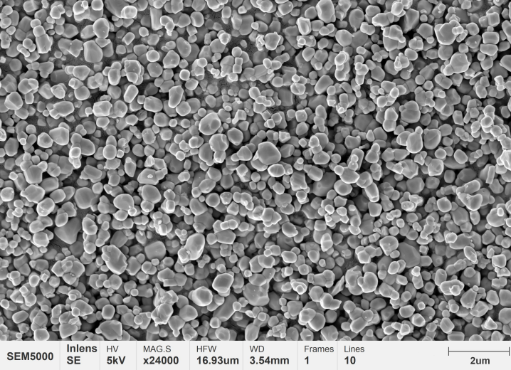
Fig.2 Microscopic morphology of barium titanate ceramic powder
Barium strontium titanate (BaxSr1-xTiO3) is also an important electronic ceramic material, which is a solid solution formed by strontium titanate and barium titanate. Compared with barium titanate, it has higher dielectric constant, lower dielectric loss, high breakdown strength and adjustable phase transition point with composition, and has been studied by many scholars and widely used in electronic devices.
At present, researchers often use methods such as adjusting the Sr/Ba ratio and doping elements to achieve the purpose of improving performance. However, it is fundamental to adjust the material properties by changing the microstructure of the material. Figure 3 is the backscattered electron image of the barium strontium titanate sintered product tested by the field emission scanning electron microscope SEM5000. It can be used to characterize the composition uniformity of the material at low magnification. At the same time, the backscattered electron image at high magnification also has a certain shape contrast.
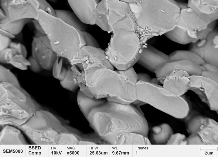
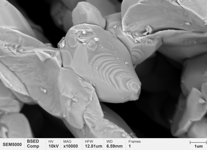
Fig.3 Microscopic morphology of barium strontium titanate sintered product
Ceramic materials, metal materials, and polymer materials are the three most widely used materials in today’s society. With the continuous development of science and technology and the social economy, more stringent requirements will be put forward on the performance of ceramic materials in the future. The use of scanning electron microscopy to characterize the microstructure of ceramic materials will help improve the preparation technology of ceramic materials and move towards a higher level. performance development.
Field Emission Scanning Electron Microscope SEM5000
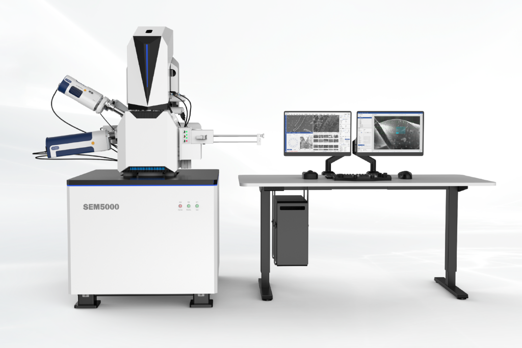
SEM5000 is a field emission scanning electron microscope with high resolution and rich functions. It has an advanced lens barrel design, deceleration inside the lens barrel, low aberration, and no magnetic leakage objective lens design, which realizes low-voltage high-resolution imaging and is applicable to on magnetic samples. SEM5000 has optical navigation, complete automatic functions, well-designed human-computer interaction, and optimized operation and use process. No matter whether the operator has rich experience or not, he can quickly get started and complete high-resolution shooting tasks.