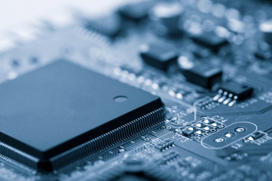
With the blowout growth of the semiconductor industry in recent years, the use of scanning electron microscopes in key technologies has also received unprecedented attention. Nowadays, the operation and maintenance of desktop electron microscopes are becoming easier and easier, which undoubtedly increases the research and development, and production of domestic semiconductor manufacturers. As a sharp tool, the current desktop scanning electron microscope is mainly used in the semiconductor industry for morphology observation, and more importantly, for elemental analysis.
The development of nanotechnology leads to the rapid development of nanoscale manufacturing, and nanofabrication is the core part of nanomanufacturing. The representative method of nanofabrication is a focused ion beam.
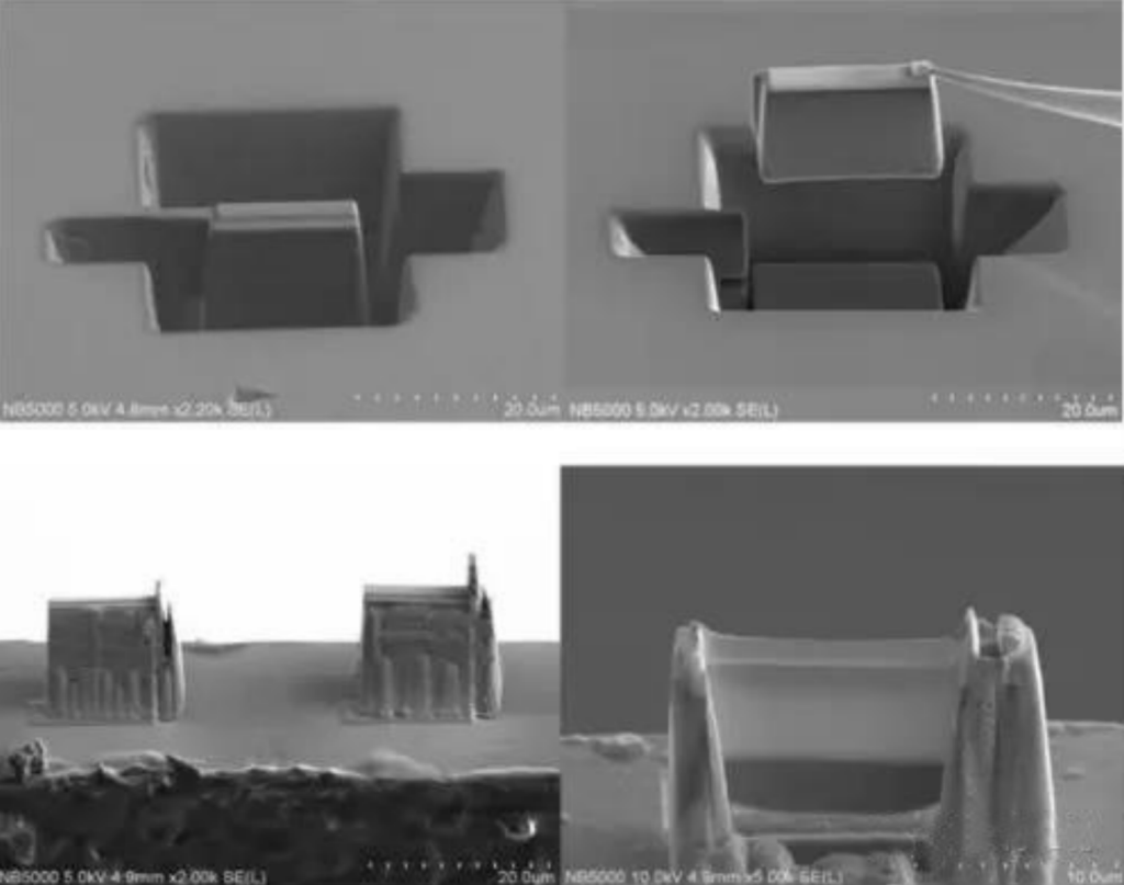
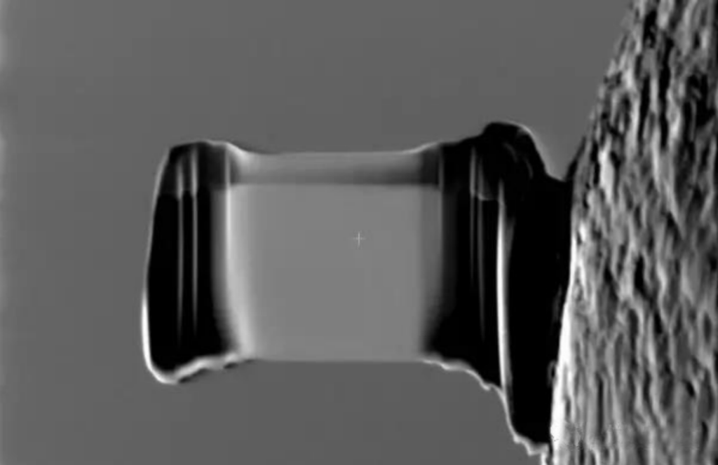
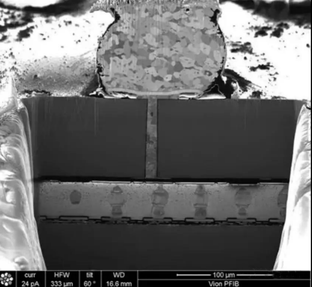
The Focused Ion Beam (FIB) technology developed in recent years uses high-intensity focused ion beams for nano processing of materials, combined with scanning electron microscopy (SEM) and other high-power electron microscopes for real-time observation, and has become the main method for nanoscale analysis and manufacturing. At present, it is widely used in semiconductor integrated circuit modification, cutting and fault analysis, TEM sample preparation, etc.
Function and use:
The use of high-intensity focused ion beams for nano processing of materials, combined with scanning electron microscopy (SEM) and other high-magnification electron microscopes for real-time observation, has become the main method for nanoscale analysis and manufacturing.
Applicable areas include:
- IC chip circuit modification
- Cross-Section section analysis
- Probing Pad
- FIB TEM sample preparation
- Material identification and other fields.
FIB-SEM technology was used to cut off the electrode coating layer by layer every 500nm to obtain 160 cross-sectional photos, and then reconstruct the three-dimensional microstructure of the electrode. The pixel resolution of the reconstructed structure is 500nm, which is relatively high, and the resolution of general XCT technology is about 1 μm. The binder and conductive agent particles are too small to be distinguished, so they are regarded as a mixed phase (carbon colloidal phase).
In the figure-reconstruction of the microstructure of the electrode coating: (a) cross-section of lithium cobalt oxide electrode, (b) cross-section of graphite electrode, (c) three-dimensional structure reconstructed by lithium cobalt oxide, (d) three-dimensional structure reconstructed by graphite
Special applications of scanning electron microscopy in semiconductor device research:
1. Imaging using electron beam-induced current can be used for positioning and damage research in integrated circuits.
2. Using sample current imaging, the results can show the opening and short circuit of the metal layer in the circuit, so the resistance contrast image is often used to check the metal wiring layer, a polycrystalline wiring layer, metal-to-silicon test pattern and the conductive form of thin film resistance.
3. Use the secondary electron potential contrast image to reflect the potential on the surface of the sample. From it, you can see the level and distribution of the potential on the surface of the sample, especially for the determination of the hidden open circuit or hidden short circuit of the device.