In the field of materials, scanning electron microscopy plays an extremely important role and is widely used in the research of the morphology and structure of various materials, interface conditions, damage mechanisms, and material performance prediction. The scanning electron microscope can be used to directly study crystal defects and their generation process, to observe the aggregation mode of atoms inside the metal material and their real boundaries, to observe the way of boundary movement under different conditions, and to check the crystal defects caused by surface machining. damage and radiation damage.
01 Introduction to Scanning Electron Microscopy (SEM)
Scanning electron microscope (SEM) is a microscopic morphology observation method between transmission electron microscope and optical microscope, which can directly use the material properties of the sample surface material for microscopic imaging.
Advantage
- High magnification, continuously adjustable between 200,000 and 200,000 times;
- Large depth of field, large field of view, direct observation of fine structures;
- Sample preparation is simple:
- It can observe the microscopic morphology and analyze the composition of the micro-area at the same time.
02 Working Principle of Scanning Electron Microscope (SEM)
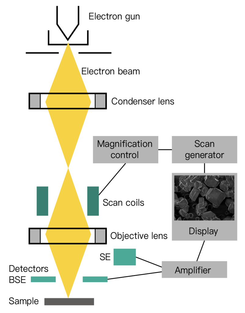
In principle, the scanning electron microscope uses a very finely focused high-energy electron beam to scan on the sample to stimulate various physical information. Observation of the surface topography of the test sample is obtained by accepting, amplifying and displaying the information.
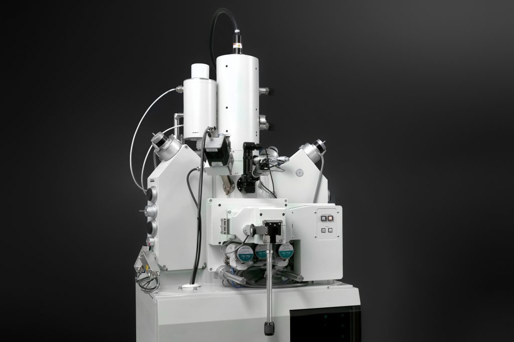
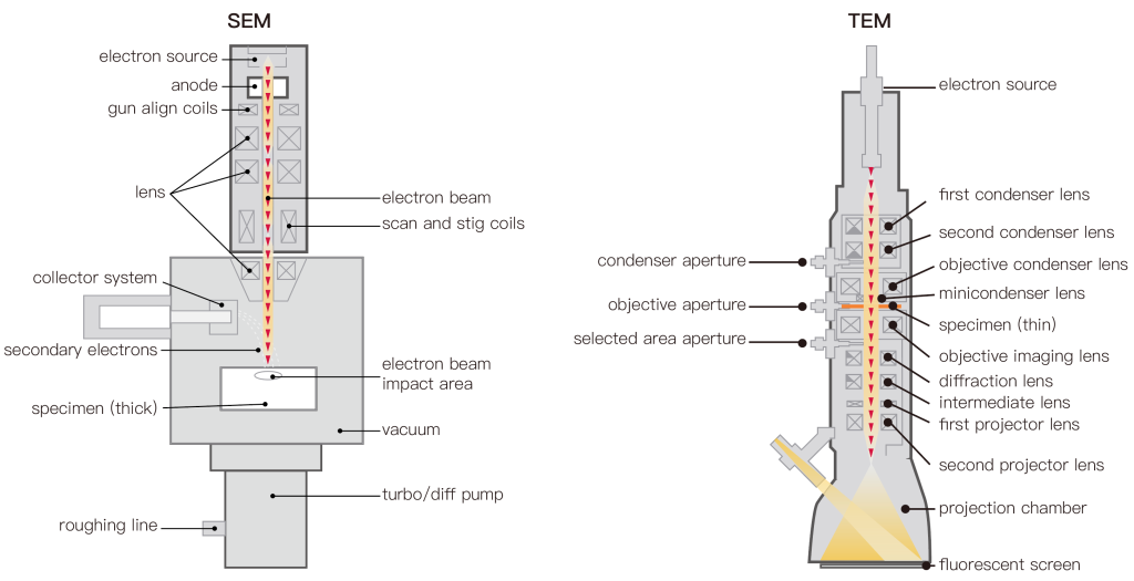
03 Construction of Scanning Electron Microscope (SEM)
SEM can be divided into three main parts:
- a. Electron optical system
- b. signal collection and processing, image display and recording system
- c. Vacuum system
Electron optical system
Function: It is used to obtain a very thin electron beam (about a few nm in diameter) as an excitation source for generating physical signals.
Electron gun, electromagnetic lens, scanning coil, sample chamber
Electron gun
Function: Use the high voltage between the cathode and the anode filament to generate a high-energy electron beam.


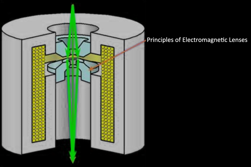
Electromagnetic lens
Condenser function: mainly to focus and shrink the beam spot (virtual light source) of the electron gun step by step, so that the original beam spot with a diameter of about 50 μm is reduced to a small beam spot with only a few nm.
Scan coil
Function: to deflect the electron beam and make a regular scan on the sample surface; that is, to provide the synchronous scanning signal of the incident electron beam on the sample surface and the electron beam in the cathode ray tube on the fluorescent screen.
Sample room
The main component is the sample stage. It can hold a sample of a certain size, and can move the sample in three-dimensional space, and can also tilt and rotate, so as to facilitate various analysis of each specific position on the sample.
Signal collection and display system
Function: Collect (detect) various physical signals generated by the sample under the action of the incident electron beam and amplify them; convert the modulated signal output by the signal detection and amplification system into an image that can be displayed on the fluorescent screen of the cathode ray tube for observation or recording .
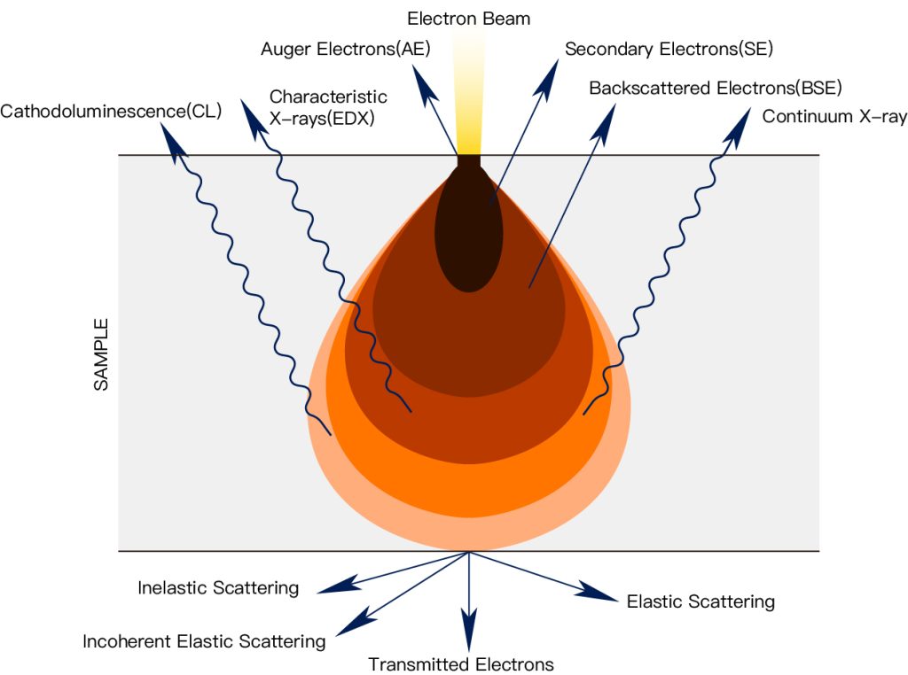
Vacuum system
Function: To ensure the normal operation of the electron optical system, prevent sample contamination, and avoid rapid decline in filament life.
It is necessary to provide a high degree of vacuum. Generally, it is required to maintain a vacuum degree of 10-4~10-5mmHg.
04 Performance Parameters of Scanning Electron Microscope (SEM)
The main performance parameters of a scanning electron microscope (SEM) are resolution and magnification.
Resolution:
For micro-area component analysis, it refers to the smallest area that can be analyzed; for imaging, it refers to the smallest distance between two points that can be resolved.
Magnification: K=As/Ac
The amplitude of synchronous scanning of As fluorescent screen anode ray, scanning amplitude of Ac electron beam on the sample surface
Comparison of the performance of various microscopes
| Microscope | OM | SEM | TEM | |
| Magnification | 1 ~ 2000 | 5 ~ 200000 | 100 ~ 80000 | |
| Resolution | Highest | 0.1μm | 0.8nm | 0.2nm |
| Skilled operation | 0.2μm | 6nm | 1nm | |
| General operation | 5μm | 10 ~ 50nm | 10nm | |
| Depth of focus | Poor, e.g. 1 μm (×100) | High, e.g. 100 μm (×100) | Moderate, e.g. 10 times smaller than SEM | |
| Field of View | Medium | Large | Small | |
| Operation and maintenance | Convenient and simple | Relatively convenient and simple | Complicated | |
| Specimen preparation | Metallographic surface technology | Any surface can be | thin film or lamination technology | |
| price | low | high | high | |
05 Scanning electron microscope (SEM) contrast image
Contrast: The brightness of the electron image depends on the strength of the electron beam. When the electron intensity in the two regions is different, there will be a difference in the brightness of the image. This difference is the contrast.
It is divided into secondary electron image contrast and backscattered electron image contrast.
Secondary electron image contrast: The extranuclear electrons that are bombarded by the incident electron beam and leave the surface of the sample are called secondary electrons, which are free electrons in vacuum.
Features of secondary electron image contrast:
●High resolution;
●Strong three-dimensional sense;
●Main reaction morphology contrast;
●Used for shape analysis of samples.
Backscattered electron image contrast: backscattered electrons are part of the incident electrons bounced back by the atomic nuclei in the solid sample, and the backscattered electrons come from the depth range of several hundred nanometers on the surface of the sample.
Features of backscattered electron image contrast:
●Low resolution;
●Low detection efficiency and low contrast;
●Main reaction atomic number contrast;
●For shape analysis and component analysis.
Secondary electron image
Backscattered electron image
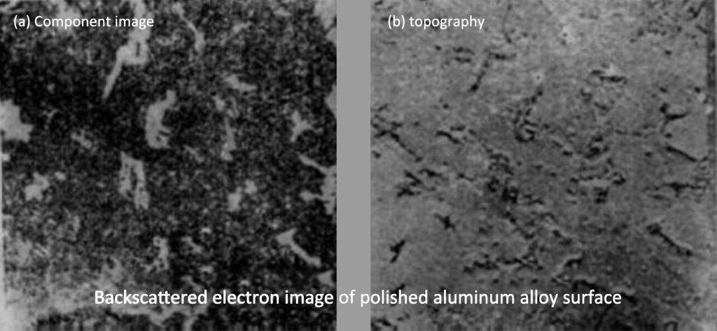
Backscattered electron image
(white: Sn; gray: Al2O3)
06 Sample preparation of Scanning Electron Microscopy (SEM)
The main requirements of scanning electron microscopy for samples are: dry, oil-free, and conductive.
Principles of sample preparation
- Morphology, must be resistant to high vacuum;
- The surface of the sample should not contain organic grease pollutants;
- The sample must be dry;
- The surface of the sample must be conductive.
Sample preparation method
bulk sample
Block conductive samples – no sample preparation is required, and the samples are bonded to the sample holder with conductive glue for direct observation.
Bulk non-conductive samples or samples with poor conductivity – Coating should be done first.
Powder specimen
Conductive powder sample – firstly bond the conductive tape to the sample holder, then evenly sprinkle the powder sample on it, blow off the non-adhesive powder with the ear washing ball, and then observe with the electron microscope.
Powdered non-conductive samples or samples with poor conductivity – a layer of conductive film should be coated before observation with an electron microscope.
Metal and Ceramic Specimen
- Morphology Observation: Thoroughly remove oil to avoid hydrocarbon contamination.
- Compositional image or atomic number contrast: When we need to study the weak contrast mechanism (the average atomic number difference between two phases is small), it is necessary to eliminate the contrast effect of the sample morphology. Polish the sample.
- WDS microscopic quantitative analysis of chemical elements: requires very smooth surface, mechanical polishing, electrolytic polishing, chemical treatment, etc.
- Metallurgical metallurgical microstructure: mechanical polishing, corrosion.
- Fracture Microanalysis: Use a low-speed diamond saw, or wire-cut sampling to minimize thermal and mechanical damage to the material.
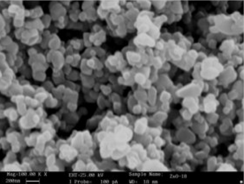
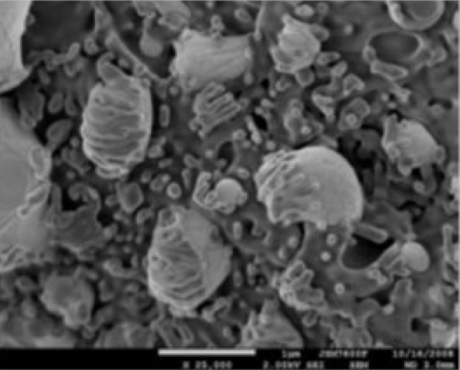
07 SEM application examples
- Observe the surface morphology of the material
It can be clearly observed from the figure that there are a large number of tear edges and tear flats on the peeling surface, and there are many small radial stripes and dimples on the tear platform.
- Observe the second phase of the material
The size of the broken second phase Mg17A12 is about 4μm, and there are many small particles dispersedly distributed near the “big” Mg17A12, the size of which is about 0.5μm. The secondary Mg17A12 phase precipitated in the
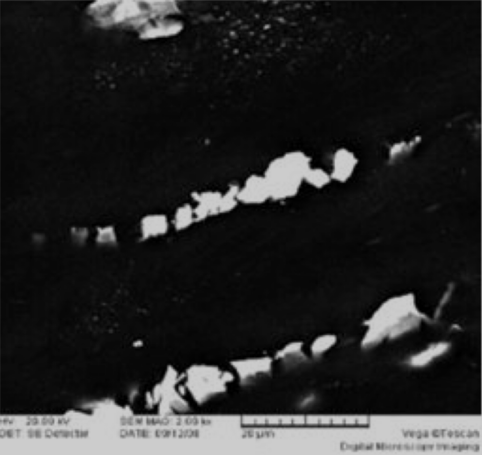
- Observe Material Interface
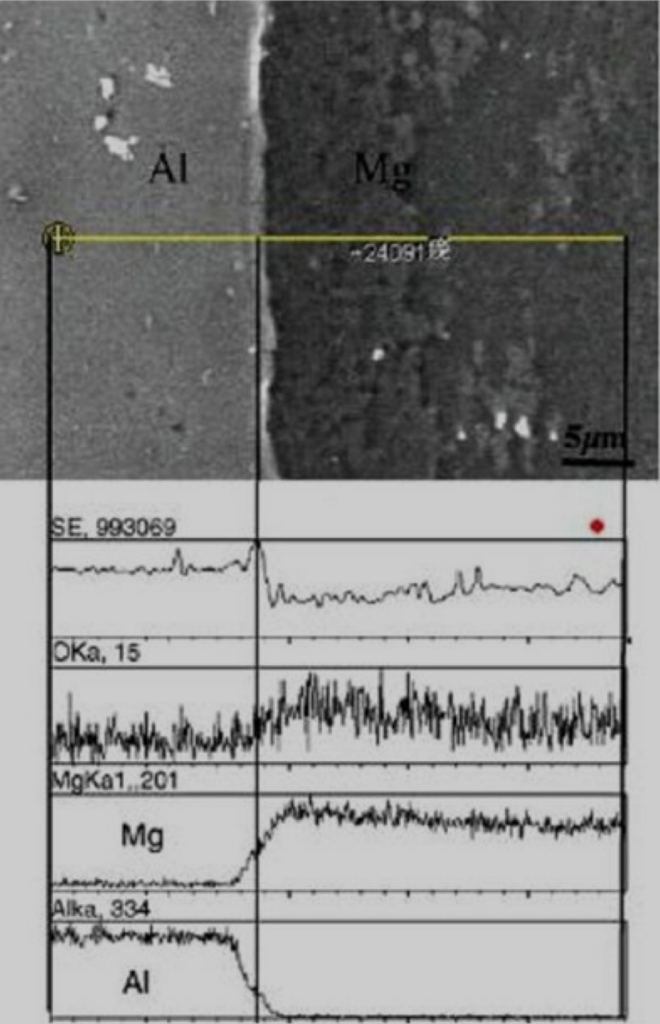
It can be seen from the figure that the line scan across the interface between Mg and Al can be obtained, on the Al side, the Mg content is low, and on the Mg side, the AI is almost zero; but at the interface, the Mg and Al are respectively Accounted for about half, indicating that diffusion occurred at the interface, forming a diffusion layer of Mg and Al.
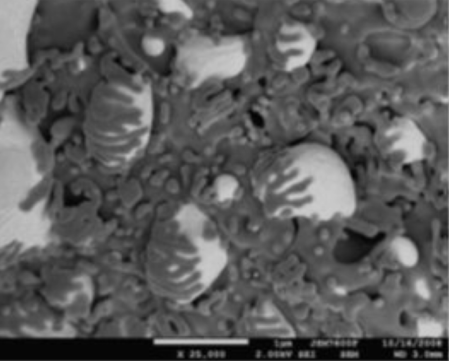
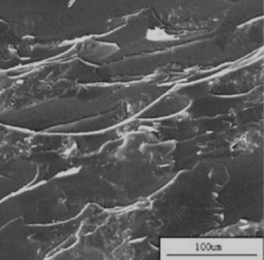
- Observe material fracture

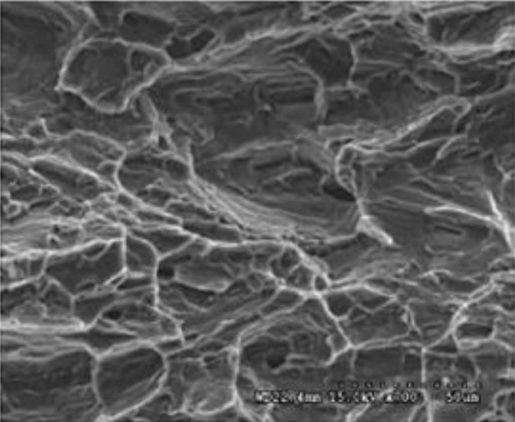
Tensile Fracture Morphology of AZ31 Magnesium Alloy
From Figure (a), it can be observed that there is an obvious cleavage fracture platform, and there are also a small amount of dimples at the final tear, which basically belongs to quasi-cleavage fracture and has poor plasticity. This is because there is a coarse brittle second phase Mg17Al12 at the grain boundary of the as-cast AZ31 magnesium alloy, which is easily broken to form a crack source during the tensile deformation process.
The hot-rolled AZ31 magnesium alloy tensile sample has an obvious necking phenomenon at the fracture site. The SEM scanning morphology of the macro-fracture is shown in Figure (b), showing the ductile fracture morphology features mainly dimples, and dimples The size is 5~20μm.