Field Emission Transmission Electron Microscope (abbreviated as TEM), referred to as TEM, is an electron optical instrument with high resolution and high magnification, which uses an electron beam with an extremely short wavelength as the illumination source and uses an electromagnetic lens to focus and image. Usually, the resolution of the field emission electron microscope is 0.1-0.2nm, and the magnification is tens of thousands to millions of times. Microstructure”. Transmission electron microscopy is mainly used to observe the microstructure of various materials and analyze samples at the nanometer scale.
The case
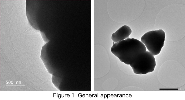
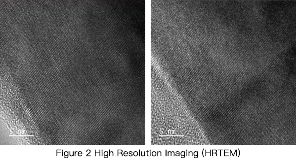
- 1. The morphology and high-resolution image (HRTEM) of a certain battery material. The particle size can be seen from the ordinary morphology, and the coating layer on the surface of the particle can be seen from the high-resolution image.
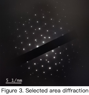
2. Selected area diffraction of battery material.
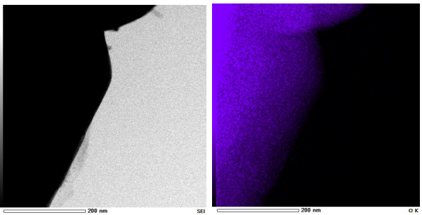
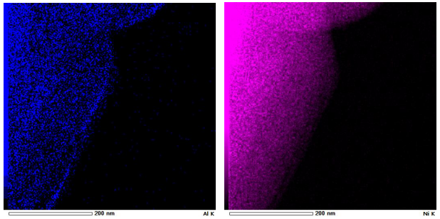
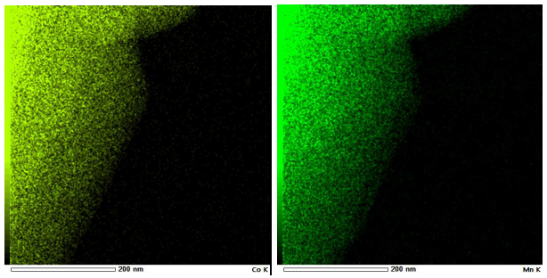
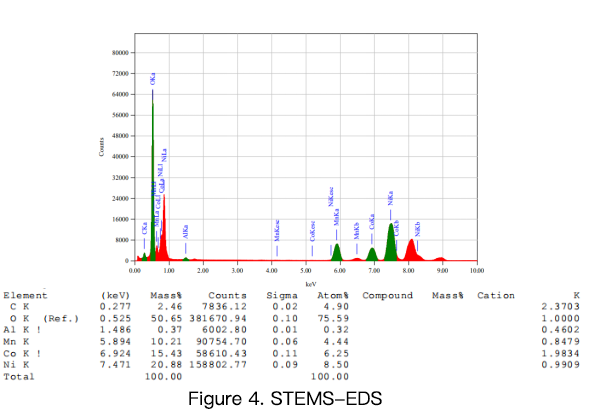
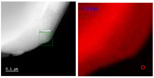
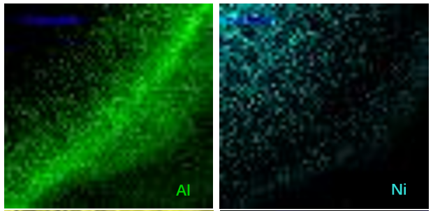
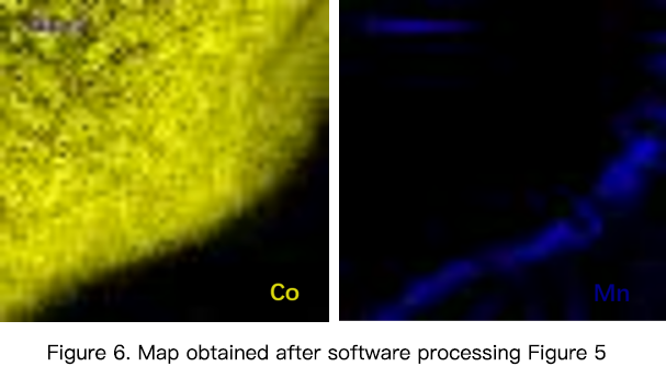
3. STEM-EDS of a certain battery material
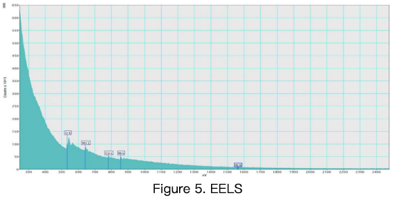
4. Electron energy loss spectrum (EELS) of a battery material
Introduction of TEM equipment in the test and analysis center
Equipment Model: Field Emission Transmission Electron Microscope
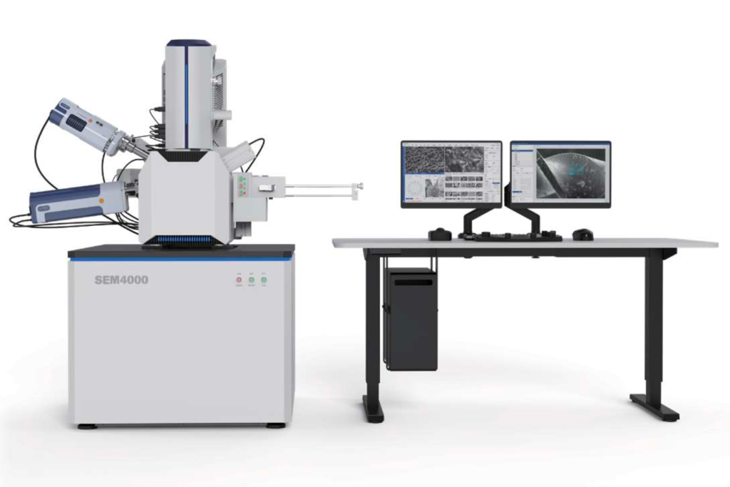
01. Equipment Introduction
It is mainly used for high-resolution morphology observation of materials, crystal structure analysis and composition analysis of micro-regions. Such as morphology observation, high-resolution electron microscopy (HRTEM), selected area electron diffraction (SAED), converging beam electron diffraction (CBED), diffraction contrast imaging (BF, DF), X-ray energy spectrum analysis (EDS) And electron energy loss spectroscopy (EELS), etc.
02. principle
The transmission electron microscope uses electrons as the illumination beam. The electrons emitted by the electron gun, under the action of the anode acceleration voltage, pass through the condenser mirror and converge into an electron beam to illuminate the sample. The electrons passing through the sample carry the structural information of the sample itself, and pass through the objective lens and the intermediate mirror. And the projection mirror is focused and enlarged, and finally displayed on the fluorescent screen in the form of an image or diffraction spectrum.
03. application
Observation of the internal microstructure of various materials, electron diffraction analysis and high-resolution electron microscopy research, research on crystal structure and crystal properties, and energy spectrometer can be used to conduct qualitative and semi-quantitative micro-region analysis of various elements Analysis, widely used in nanotechnology, materials, physics, biology, chemistry, environment, optoelectronics and other fields.
04. Instrument Features
- 1. Point resolution: 0.19nm;
- 2. Line resolution: 0.10nm;
- 3. Acceleration voltage: up to 200kV;
- 4. Magnification: TEM mode: 50~2M×; STEM mode: 200~150M×;
- 5. STEM resolution: ≤0.16nm;
- 6. Equipped with a five-axis motor-driven fully automatic sample stage, and the manual replacement method coexists at the same time;
- 7. Dual-energy spectrum probe;
- 8. Electron energy loss spectrometer components.